 |
Motore di ricerca datesheet componenti elettronici |
|
|
Motore di ricerca datesheet componenti elettronici |
|
The question interval is too short.
Please try again in a few seconds.

Hello, Please ask a question about FP5101 Datasheet
# Example questions:
➢ What are the key considerations when selecting an inductor, beyond simply calculating the required inductance value, as described in the 'inductor selection' section?
➢ What happens to the current stress on the input capacitor when the output voltage (vout) is half of the input voltage (vin)?
➢ What is a recommended range for the inductor ripple current as a percentage of the maximum load current?
| Part No. | FP5101 |
| Manufacturer | FEELING |
| Size | 734 Kbytes |
| Pages | 20 pages |
| Description | 1 Channel Synchronous PWM Controller |

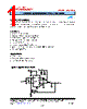
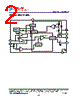
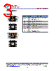
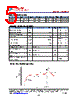
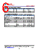
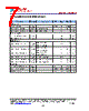
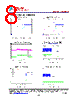


1. Overview & Function
️· FP5101/FP5101A: A power IC designed for DC-DC conversion, likely a buck converter configuration (based on the terminology used).
️· Focus: The document details considerations for selecting external components (capacitors and inductors) to ensure optimal performance and stability.
️· Compensation: A significant portion of the document is devoted to designing the compensation network to achieve a stable control loop for the converter.
2. Input Capacitor Selection
️· Voltage Rating: The input capacitor's voltage rating should be 1.25-1.5 times the *maximum* input voltage, with a more conservative approach suggesting up to 2 times the maximum voltage. This is crucial to handle voltage stress and transients.
️· RMS Current Handling: The capacitor needs to handle the RMS current, which is influenced by the input voltage and output voltage. The datasheet mentions that the worst-case RMS current stress is when the output voltage is half the input voltage.
️· Type: A low-ESR (Equivalent Series Resistance) capacitor is required for good high-frequency decoupling. Ceramic capacitors are commonly used for this purpose.
3. Inductor Selection
️· Ripple Current: The inductor value is selected to manage the inductor ripple current. A larger inductor value leads to lower ripple current, but also increases inductor size and series resistance. A good starting point is to keep the ripple current at 10-20% of the maximum load current.
️· Inductance Calculation:
- L = [(V<sub>IN</sub> - V<sub>OUT</sub>) * V<sub>OUT</sub>] / (f * ΔI) (where: V<sub>IN</sub> = Input Voltage, V<sub>OUT</sub> = Output Voltage, f = Switching Frequency, ΔI = Ripple Current)
️· Ripple Current Calculation:
* ΔI = [(V<sub>IN</sub> - V<sub>OUT</sub>) * V<sub>OUT</sub>] / (f * L)
️· Saturation: The inductor must be chosen to avoid saturation under the *worst-case* operating conditions (maximum load and highest temperature). Consider the peak inductor current: I<sub>L_PEAK</sub> = I<sub>O</sub> + ΔI/2.
️· Where:
* I<sub>O</sub> = Output current
* ΔI = ripple current
4. Compensation Network Design
️· Purpose: The compensation network stabilizes the control loop, prevents oscillations, and optimizes transient response.
️· General Strategy:
1. Gain Selection: Choose a gain (R<sub>2</sub>/R<sub>1</sub>) based on the desired bandwidth.
2. Zero Placement: Place the first zero (Z1) at 0.75 times the filter's double pole frequency (F<sub>LC</sub>).
3. Pole Placement: Place the first pole (P1) at the filter's ESR (Equivalent Series Resistance) zero. Place the second pole (P2) at half the switching frequency (0.5 * F<sub>S</sub>).
4. Where:
■ F<sub>S</sub> = Switching frequency
5. Gain Check: Verify that the compensation gain is compatible with the open-loop error amplifier gain.
6. Phase Margin: Aim for a phase margin greater than 45 degrees.
1. Overview & Function
️· FP5101/FP5101A: A power IC designed for DC-DC conversion, likely a buck converter configuration (based on the terminology used).
️· Focus: The document details considerations for selecting external components (capacitors and inductors) to ensure optimal performance and stability.
️· Compensation: A significant portion of the document is devoted to designing the compensation network to achieve a stable control loop for the converter.
2. Input Capacitor Selection
️· Voltage Rating: The input capacitor's voltage rating should be 1.25-1.5 times the *maximum* input voltage, with a more conservative approach suggesting up to 2 times the maximum voltage. This is crucial to handle voltage stress and transients.
️· RMS Current Handling: The capacitor needs to handle the RMS current, which is influenced by the input voltage and output voltage. The datasheet mentions that the worst-case RMS current stress is when the output voltage is half the input voltage.
️· Type: A low-ESR (Equivalent Series Resistance) capacitor is required for good high-frequency decoupling. Ceramic capacitors are commonly used for this purpose.
3. Inductor Selection
️· Ripple Current: The inductor value is selected to manage the inductor ripple current. A larger inductor value leads to lower ripple current, but also increases inductor size and series resistance. A good starting point is to keep the ripple current at 10-20% of the maximum load current.
️· Inductance Calculation:
- L = [(V<sub>IN</sub> - V<sub>OUT</sub>) * V<sub>OUT</sub>] / (f * ΔI) (where: V<sub>IN</sub> = Input Voltage, V<sub>OUT</sub> = Output Voltage, f = Switching Frequency, ΔI = Ripple Current)
️· Ripple Current Calculation:
* ΔI = [(V<sub>IN</sub> - V<sub>OUT</sub>) * V<sub>OUT</sub>] / (f * L)
️· Saturation: The inductor must be chosen to avoid saturation under the *worst-case* operating conditions (maximum load and highest temperature). Consider the peak inductor current: I<sub>L_PEAK</sub> = I<sub>O</sub> + ΔI/2.
️· Where:
* I<sub>O</sub> = Output current
* ΔI = ripple current
4. Compensation Network Design
️· Purpose: The compensation network stabilizes the control loop, prevents oscillations, and optimizes transient response.
️· General Strategy:
1. Gain Selection: Choose a gain (R<sub>2</sub>/R<sub>1</sub>) based on the desired bandwidth.
2. Zero Placement: Place the first zero (Z1) at 0.75 times the filter's double pole frequency (F<sub>LC</sub>).
3. Pole Placement: Place the first pole (P1) at the filter's ESR (Equivalent Series Resistance) zero. Place the second pole (P2) at half the switching frequency (0.5 * F<sub>S</sub>).
4. Where:
■ F<sub>S</sub> = Switching frequency
5. Gain Check: Verify that the compensation gain is compatible with the open-loop error amplifier gain.
6. Phase Margin: Aim for a phase margin greater than 45 degrees.
| Part No. | FP5101 |
| Manufacturer | FEELING |
| Size | 734 Kbytes |
| Pages | 20 pages |
| Description | 1 Channel Synchronous PWM Controller |
| Lei ha avuto il aiuto da alldatasheet? [ DONATE ] |
Di alldatasheet | Richest di pubblicita | contatti | Privacy Policy | Collegamento alla scheda tecnica | scambio Link | Ricerca produttore All Rights Reserved©Alldatasheet.com |
| Russian : Alldatasheetru.com | Korean : Alldatasheet.co.kr | Spanish : Alldatasheet.es | French : Alldatasheet.fr | Italian : Alldatasheetit.com Portuguese : Alldatasheetpt.com | Polish : Alldatasheet.pl | Vietnamese : Alldatasheet.vn Indian : Alldatasheet.in | Mexican : Alldatasheet.com.mx | British : Alldatasheet.co.uk | New Zealand : Alldatasheet.co.nz |
|
Family Site : ic2ic.com |
icmetro.com |
 Italian ▼
  English
 Chinese
 German
 Japanese
 Russian
 Korean
 Spanish
 French
 Portuguese
 Polish
 Vietnamese
 Indian
 Mexican
 British
 New Zealand