 |
Motore di ricerca datesheet componenti elettronici |
|
|
Motore di ricerca datesheet componenti elettronici |
|
The question interval is too short.
Please try again in a few seconds.

Hello, Please ask a question about GD25LE40CNEG Datasheet
# Example questions:
➢ What happens to the protected memory area size for gd25le40c when the cmp bit in the status register is set to 1?
➢ If you want to protect the entire memory area of a gd25le20c flash chip using the status register bits bp4-bp0, what values should you set for those bits?
➢ Comparing table 1 and table 2, what is a key difference in how the protected area sizes are defined for the gd25le40c versus the gd25le20c flash chips?
| Part No. | GD25LE40CNEG |
| Manufacturer | GIGADEVICE |
| Size | 1Mb |
| Pages | 75 pages |
| Description | 1.8V Uniform Sector Dual and Quad Serial Flash |




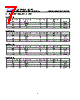




1. Understanding Block Protect (BP) Bits
️· Purpose: The Block Protect (BP) bits in the status register determine which blocks of flash memory are write-protected. This helps prevent accidental or unauthorized modifications to specific areas of the flash.
️· Status Register: The BP bits are part of the device's status register, which can be read and written to configure the memory's protection.
️· CMP Bit: The "CMP" bit (Compare) determines how the BP bits are interpreted. This is crucial; the interpretation *completely* changes the protection zones. I'm including this because it is mentioned at the end of each table.
2. GD25LE40C - Protection Schemes (CMP=0)
️· Interpretation: When CMP = 0, the BP bits define protection zones based on specific block numbers. It is a more granular block based protection.
️· Main Groups: The blocks are grouped in multiples of 4kb, 8kb and 16kb.
- Bottom Block Protection (1110, 1111): The lower most blocks are protected. The number of protected blocks depends on the exact BP combination.
- Upper Block Protection (1000, 1001, 1010, 1011): Protecting blocks starting from the upper addresses of the device.
️· Protection Zones: A large number of zones are possible, with the protection regions based on which combination of BP bits are set. Refer to the table for the specific addresses.
3. GD25LE40C - Protection Schemes (CMP=1)
️· Interpretation: When CMP = 1, the BP bits indicate the *start* of the protected region. Protection extends to the end of the flash memory. It provides a less granular, wider area protection.
️· Protection Zones: The tables describe the start addresses and the areas that are protected.
️· Simpler Configuration: This mode is generally simpler to configure as it provides broader protection.
4. GD25LE20C - Protection Schemes (CMP=0)
️· Similar to GD25LE40C: This device has a similar concept where the status register bits determine which blocks of flash memory are write-protected.
️· Smaller Flash Capacity: Compared to the GD25LE40C, the protection ranges are smaller due to the smaller flash capacity.
️· Interpreted Based on BP Bit Combination: The specific addresses of protected blocks change based on the combination of BP bits set in the status register.
Key Differences Between Devices
| Feature | GD25LE40C | GD25LE20C |
|---|---|---|
| Flash Capacity | Larger | Smaller |
| Granularity of Protection (CMP=0) | Higher, more precise block-level protection | Similar, but limited by smaller flash capacity |
| CMP=1: | Broader Protection | Similar |
1. Understanding Block Protect (BP) Bits
️· Purpose: The Block Protect (BP) bits in the status register determine which blocks of flash memory are write-protected. This helps prevent accidental or unauthorized modifications to specific areas of the flash.
️· Status Register: The BP bits are part of the device's status register, which can be read and written to configure the memory's protection.
️· CMP Bit: The "CMP" bit (Compare) determines how the BP bits are interpreted. This is crucial; the interpretation *completely* changes the protection zones. I'm including this because it is mentioned at the end of each table.
2. GD25LE40C - Protection Schemes (CMP=0)
️· Interpretation: When CMP = 0, the BP bits define protection zones based on specific block numbers. It is a more granular block based protection.
️· Main Groups: The blocks are grouped in multiples of 4kb, 8kb and 16kb.
- Bottom Block Protection (1110, 1111): The lower most blocks are protected. The number of protected blocks depends on the exact BP combination.
- Upper Block Protection (1000, 1001, 1010, 1011): Protecting blocks starting from the upper addresses of the device.
️· Protection Zones: A large number of zones are possible, with the protection regions based on which combination of BP bits are set. Refer to the table for the specific addresses.
3. GD25LE40C - Protection Schemes (CMP=1)
️· Interpretation: When CMP = 1, the BP bits indicate the *start* of the protected region. Protection extends to the end of the flash memory. It provides a less granular, wider area protection.
️· Protection Zones: The tables describe the start addresses and the areas that are protected.
️· Simpler Configuration: This mode is generally simpler to configure as it provides broader protection.
4. GD25LE20C - Protection Schemes (CMP=0)
️· Similar to GD25LE40C: This device has a similar concept where the status register bits determine which blocks of flash memory are write-protected.
️· Smaller Flash Capacity: Compared to the GD25LE40C, the protection ranges are smaller due to the smaller flash capacity.
️· Interpreted Based on BP Bit Combination: The specific addresses of protected blocks change based on the combination of BP bits set in the status register.
Key Differences Between Devices
| Feature | GD25LE40C | GD25LE20C |
|---|---|---|
| Flash Capacity | Larger | Smaller |
| Granularity of Protection (CMP=0) | Higher, more precise block-level protection | Similar, but limited by smaller flash capacity |
| CMP=1: | Broader Protection | Similar |
| Part No. | GD25LE40CNEG |
| Manufacturer | GIGADEVICE |
| Size | 1Mb |
| Pages | 75 pages |
| Description | 1.8V Uniform Sector Dual and Quad Serial Flash |
| Lei ha avuto il aiuto da alldatasheet? [ DONATE ] |
Di alldatasheet | Richest di pubblicita | contatti | Privacy Policy | Collegamento alla scheda tecnica | scambio Link | Ricerca produttore All Rights Reserved©Alldatasheet.com |
| Russian : Alldatasheetru.com | Korean : Alldatasheet.co.kr | Spanish : Alldatasheet.es | French : Alldatasheet.fr | Italian : Alldatasheetit.com Portuguese : Alldatasheetpt.com | Polish : Alldatasheet.pl | Vietnamese : Alldatasheet.vn Indian : Alldatasheet.in | Mexican : Alldatasheet.com.mx | British : Alldatasheet.co.uk | New Zealand : Alldatasheet.co.nz |
|
Family Site : ic2ic.com |
icmetro.com |
 Italian ▼
  English
 Chinese
 German
 Japanese
 Russian
 Korean
 Spanish
 French
 Portuguese
 Polish
 Vietnamese
 Indian
 Mexican
 British
 New Zealand