 |
Motore di ricerca datesheet componenti elettronici |
|
|
Motore di ricerca datesheet componenti elettronici |
|
The question interval is too short.
Please try again in a few seconds.

Hello, Please ask a question about 1340C-3 Datasheet
# Example questions:
➢ What is the primary function of the ds1340, and what type of information does it provide?
➢ Describe the power control mechanism of the ds1340, including how it switches between vcc and vbackup, and what conditions trigger these switches.
➢ What is the purpose of the ft/out pin, and how can its functionality be configured?
| Part No. | 1340C-3 |
| Manufacturer | MAXIM |
| Size | 235 Kbytes |
| Pages | 14 pages |
| Description | I2C RTC with Trickle Charger |

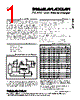


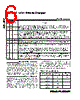


1. General Overview
️· Device: DS1340 Real-Time Clock / Calendar
️· Communication: Uses the I²C (I-squared C) serial communication protocol.
️· Functionality: Provides timekeeping (seconds, minutes, hours, day, date, month, year) and calendar functions, including automatic date adjustments and leap year correction.
️· Low Power: Designed for low power consumption.
️· Power Sense: Includes a power sense circuit to detect power failures and switch to a backup power supply.
2. Power Management
️· VCC & VBACKUP: Operates with two power supplies:
- VCC: Primary power supply.
- VBACKUP: Backup power supply (e.g., a coin cell battery or supercapacitor).
️· Power-Sense Threshold (VPF): Critical voltage level. Read/write access is blocked when VCC falls below VPF.
️· Switching to Backup:
- If VCC < VPF and VCC < VBACKUP: The device switches to VBACKUP, and read/write access is blocked.
- If VCC < VPF and VCC > VBACKUP: Read/write access is blocked (VCC still above VBACKUP).
- If VCC > VPF and VCC < VBACKUP: Read/write access is allowed (running on VCC).
- If VCC > VPF and VCC > VBACKUP: Read/write access is allowed (running on VCC).
️· Trickle Charger: The device has a trickle charger to keep a backup battery (like a coin cell) charged when VCC is available.
️· tREC: A time delay (tREC) is required after VCC returns above VPF before read/write access is re-enabled.
3. I²C Interface
️· SDA: Serial Data Input/Output (open-drain, requires an external pull-up resistor).
️· SCL: Serial Clock Input.
️· Address: The I²C address is not explicitly given in this extract, so it's not possible to determine the address.
4. Pin Descriptions
| Pin | Description |
|---|---|
| X1/X2 | Connections for the crystal oscillator (32.768kHz). Can also be connected to an external oscillator. |
| VBACKUP | Connection for the backup power supply. |
| GND | Ground |
| SDA | Serial Data Input/Output |
| SCL | Serial Clock Input |
| FT/OUT | Frequency Test/Output: can output 512Hz signal or the OUT bit's value. Requires external pull-up resistor. |
| VCC | Primary Power Supply. Read/write access blocked below VPF. |
| N.C. | No Connection (must be connected to ground) |
1. General Overview
️· Device: DS1340 Real-Time Clock / Calendar
️· Communication: Uses the I²C (I-squared C) serial communication protocol.
️· Functionality: Provides timekeeping (seconds, minutes, hours, day, date, month, year) and calendar functions, including automatic date adjustments and leap year correction.
️· Low Power: Designed for low power consumption.
️· Power Sense: Includes a power sense circuit to detect power failures and switch to a backup power supply.
2. Power Management
️· VCC & VBACKUP: Operates with two power supplies:
- VCC: Primary power supply.
- VBACKUP: Backup power supply (e.g., a coin cell battery or supercapacitor).
️· Power-Sense Threshold (VPF): Critical voltage level. Read/write access is blocked when VCC falls below VPF.
️· Switching to Backup:
- If VCC < VPF and VCC < VBACKUP: The device switches to VBACKUP, and read/write access is blocked.
- If VCC < VPF and VCC > VBACKUP: Read/write access is blocked (VCC still above VBACKUP).
- If VCC > VPF and VCC < VBACKUP: Read/write access is allowed (running on VCC).
- If VCC > VPF and VCC > VBACKUP: Read/write access is allowed (running on VCC).
️· Trickle Charger: The device has a trickle charger to keep a backup battery (like a coin cell) charged when VCC is available.
️· tREC: A time delay (tREC) is required after VCC returns above VPF before read/write access is re-enabled.
3. I²C Interface
️· SDA: Serial Data Input/Output (open-drain, requires an external pull-up resistor).
️· SCL: Serial Clock Input.
️· Address: The I²C address is not explicitly given in this extract, so it's not possible to determine the address.
4. Pin Descriptions
| Pin | Description |
|---|---|
| X1/X2 | Connections for the crystal oscillator (32.768kHz). Can also be connected to an external oscillator. |
| VBACKUP | Connection for the backup power supply. |
| GND | Ground |
| SDA | Serial Data Input/Output |
| SCL | Serial Clock Input |
| FT/OUT | Frequency Test/Output: can output 512Hz signal or the OUT bit's value. Requires external pull-up resistor. |
| VCC | Primary Power Supply. Read/write access blocked below VPF. |
| N.C. | No Connection (must be connected to ground) |
| Part No. | 1340C-3 |
| Manufacturer | MAXIM |
| Size | 235 Kbytes |
| Pages | 14 pages |
| Description | I2C RTC with Trickle Charger |
| Lei ha avuto il aiuto da alldatasheet? [ DONATE ] |
Di alldatasheet | Richest di pubblicita | contatti | Privacy Policy | Collegamento alla scheda tecnica | scambio Link | Ricerca produttore All Rights Reserved©Alldatasheet.com |
| Russian : Alldatasheetru.com | Korean : Alldatasheet.co.kr | Spanish : Alldatasheet.es | French : Alldatasheet.fr | Italian : Alldatasheetit.com Portuguese : Alldatasheetpt.com | Polish : Alldatasheet.pl | Vietnamese : Alldatasheet.vn Indian : Alldatasheet.in | Mexican : Alldatasheet.com.mx | British : Alldatasheet.co.uk | New Zealand : Alldatasheet.co.nz |
|
Family Site : ic2ic.com |
icmetro.com |
 Italian ▼
  English
 Chinese
 German
 Japanese
 Russian
 Korean
 Spanish
 French
 Portuguese
 Polish
 Vietnamese
 Indian
 Mexican
 British
 New Zealand