 |
Motore di ricerca datesheet componenti elettronici |
|
|
Motore di ricerca datesheet componenti elettronici |
|
The question interval is too short.
Please try again in a few seconds.

Hello, Please ask a question about XC2365_08 Datasheet
# Example questions:
➢ What is the function of a 'sclkout' pin related to these channels?
➢ What are the primary functions of pins 20 and 21?
➢ What does 't3eud' represent and how is it used in relation to gpt1?
| Part No. | XC2365_08 |
| Manufacturer | INFINEON |
| Size | 1Mb |
| Pages | 112 pages |
| Description | 16/32-Bit Single-Chip Microcontroller with 32-Bit Performance |



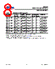
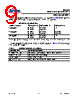


1. Device Identification
️· This is a datasheet for a microcontroller/microprocessor from Infineon (likely within their TriCore family, though not explicitly stated). The exact part number isn't given.
2. Key Features (Extracted from the Table & General Information)
️· Pin Descriptions: The datasheet provides a very detailed description of each pin on the chip. It outlines the pin's name, control register assignments (like 'O0' for output, 'I' for input), type (In, Out, PS - power supply), and function (e.g., analog input, shift data output, clock output, test data input).
️· Analog Input Channels: The chip has two Analog-to-Digital Converters (ADCs), ADC0 and ADC1, each with multiple input channels (e.g., ADC1_CH0, ADC0_CH2).
️· Timers/Counters: Multiple GPT (General Purpose Timer) modules are present (GPT1, GPT2) with associated input and output pins (e.g., T6IN, T3OUT). There's also CCU60 (Comparable Control Unit) with control inputs.
️· USIC (Universal Serial Interface Controller): The chip has USIC modules (USIC0, USIC1), designed for serial communication, with pins for shift data input/output and clock output.
️· JTAG Interface: A Joint Test Action Group (JTAG) interface is present for debugging and testing. Pins like TDI_A, TDO_A, TMS_A, and TCK_A are used for this.
️· Power Supply: Designated pins for reference voltage (_V_AREF) and reference ground (_V_AGND) for the ADCs.
️· Clocking: Pins for programmable clock signal output (EXTCLK), external clock input (BRKIN_C).
️· OCDS Break Signals: Break signals for On-Chip Debugging System.
️· Reference Voltages: Dedicated reference voltage input/ground pins (_V_AREF and _V_AGND)
3. Pin-Out Details (Summarized)
The core of the datasheet is the table detailing each pin. Here's a *partial* summary, reflecting the range of functions seen. Note: The "Ctrl." column refers to the control register associated with the pin (e.g., 'O0' means output, 'I' means input).
| Pin Number | Pin Name | Ctrl | Type | Function |
|---|---|---|---|---|
| 6 | T6OUT | O2 | St/B | GPT2 Timer T6 Toggle Latch Output |
| 7 | U0C1_DOUT | O2 | St/B | USIC0 Channel 1 Shift Data Output |
| 9 | U0C1_SCLKOUT | O3 | St/B | USIC0 Channel 1 Shift Clock Output |
| 11 | ADC0_CH0 | I | St/A | Analog Input Channel 0 for ADC0 |
| 15 | ADC1_CH0 | I | In/A | Analog Input Channel 0 for ADC1 |
| 23 | ADC0_CH2 | I | In/A | Analog Input Channel 2 for ADC0 |
| 28 | ADC0_CH4 | I | In/A | Analog Input Channel 4 for ADC0 |
| 29 | ADC0_CH5 | I | In/A | Analog Input Channel 5 for ADC0 |
1. Device Identification
️· This is a datasheet for a microcontroller/microprocessor from Infineon (likely within their TriCore family, though not explicitly stated). The exact part number isn't given.
2. Key Features (Extracted from the Table & General Information)
️· Pin Descriptions: The datasheet provides a very detailed description of each pin on the chip. It outlines the pin's name, control register assignments (like 'O0' for output, 'I' for input), type (In, Out, PS - power supply), and function (e.g., analog input, shift data output, clock output, test data input).
️· Analog Input Channels: The chip has two Analog-to-Digital Converters (ADCs), ADC0 and ADC1, each with multiple input channels (e.g., ADC1_CH0, ADC0_CH2).
️· Timers/Counters: Multiple GPT (General Purpose Timer) modules are present (GPT1, GPT2) with associated input and output pins (e.g., T6IN, T3OUT). There's also CCU60 (Comparable Control Unit) with control inputs.
️· USIC (Universal Serial Interface Controller): The chip has USIC modules (USIC0, USIC1), designed for serial communication, with pins for shift data input/output and clock output.
️· JTAG Interface: A Joint Test Action Group (JTAG) interface is present for debugging and testing. Pins like TDI_A, TDO_A, TMS_A, and TCK_A are used for this.
️· Power Supply: Designated pins for reference voltage (_V_AREF) and reference ground (_V_AGND) for the ADCs.
️· Clocking: Pins for programmable clock signal output (EXTCLK), external clock input (BRKIN_C).
️· OCDS Break Signals: Break signals for On-Chip Debugging System.
️· Reference Voltages: Dedicated reference voltage input/ground pins (_V_AREF and _V_AGND)
3. Pin-Out Details (Summarized)
The core of the datasheet is the table detailing each pin. Here's a *partial* summary, reflecting the range of functions seen. Note: The "Ctrl." column refers to the control register associated with the pin (e.g., 'O0' means output, 'I' means input).
| Pin Number | Pin Name | Ctrl | Type | Function |
|---|---|---|---|---|
| 6 | T6OUT | O2 | St/B | GPT2 Timer T6 Toggle Latch Output |
| 7 | U0C1_DOUT | O2 | St/B | USIC0 Channel 1 Shift Data Output |
| 9 | U0C1_SCLKOUT | O3 | St/B | USIC0 Channel 1 Shift Clock Output |
| 11 | ADC0_CH0 | I | St/A | Analog Input Channel 0 for ADC0 |
| 15 | ADC1_CH0 | I | In/A | Analog Input Channel 0 for ADC1 |
| 23 | ADC0_CH2 | I | In/A | Analog Input Channel 2 for ADC0 |
| 28 | ADC0_CH4 | I | In/A | Analog Input Channel 4 for ADC0 |
| 29 | ADC0_CH5 | I | In/A | Analog Input Channel 5 for ADC0 |
| Part No. | XC2365_08 |
| Manufacturer | INFINEON |
| Size | 1Mb |
| Pages | 112 pages |
| Description | 16/32-Bit Single-Chip Microcontroller with 32-Bit Performance |
| Lei ha avuto il aiuto da alldatasheet? [ DONATE ] |
Di alldatasheet | Richest di pubblicita | contatti | Privacy Policy | Collegamento alla scheda tecnica | scambio Link | Ricerca produttore All Rights Reserved©Alldatasheet.com |
| Russian : Alldatasheetru.com | Korean : Alldatasheet.co.kr | Spanish : Alldatasheet.es | French : Alldatasheet.fr | Italian : Alldatasheetit.com Portuguese : Alldatasheetpt.com | Polish : Alldatasheet.pl | Vietnamese : Alldatasheet.vn Indian : Alldatasheet.in | Mexican : Alldatasheet.com.mx | British : Alldatasheet.co.uk | New Zealand : Alldatasheet.co.nz |
|
Family Site : ic2ic.com |
icmetro.com |
 Italian ▼
  English
 Chinese
 German
 Japanese
 Russian
 Korean
 Spanish
 French
 Portuguese
 Polish
 Vietnamese
 Indian
 Mexican
 British
 New Zealand