 |
Motore di ricerca datesheet componenti elettronici |
|
|
Motore di ricerca datesheet componenti elettronici |
|
The question interval is too short.
Please try again in a few seconds.

Hello, Please ask a question about SL74HC05 Datasheet
# Example questions:
➢ What is the primary function of the open-drain outputs on the sl74hc05 chip, and why might a designer choose to use this type of output?
➢ What is the recommended operating temperature range for the sl74hc05, and what happens to the power dissipation derating if the operating temperature falls outside this range?
➢ What is the maximum input leakage current (iin) when vin = vcc or gnd, and at what supply voltage (vcc) is this specified?
| Part No. | SL74HC05 |
| Manufacturer | SLS |
| Size | 35 Kbytes |
| Pages | 5 pages |
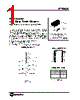
| Description | Hex Inverter with Open-Drain Outputs |


## SL74HC05 Hex Inverting Buffer Datasheet Summary
This document details the SL74HC05, a hex inverting buffer IC. Here’s a breakdown of the key information:
1. Core Functionality:
️· Type: Hex Inverting Buffer (6 independent inverters)
️· Output Type: Open-drain, requiring pull-up resistors for standard logic levels.
️· Interfaces: Designed to interface with CMOS, NMOS, and TTL logic families.
2. Electrical Characteristics:
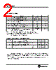
️· Supply Voltage (VCC): 2.0V to 6.0V
️· Input Logic Levels:
- VIH (Minimum High Input Voltage): 1.5V (at 2.0V VCC), 3.15V (at 4.5V VCC), 4.2V (at 6.0V VCC)
- VIL (Maximum Low Input Voltage): 0.5V (at 2.0V VCC), 1.35V (at 4.5V VCC), 1.8V (at 6.0V VCC)
️· Output Logic Levels (Low-Level): Typically around 0.1V - 0.4V depending on VCC and load current.
️· Quiescent Supply Current (ICC): 1.0µA (typical)
️· Input Leakage Current (IIN): ±1.0µA
3. AC Performance (Typical - values depend on VCC and load):
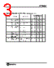
️· Propagation Delay (tPLZ, tPZL): As low as 20ns at 6V VCC.
️· Output Transition Time (tTHL): Around 13ns at 6V VCC.
4. Key Features:
️· Open-Drain Outputs: This allows for wired-OR and other custom logic configurations. Requires external pull-up resistors to function as standard logic outputs.
️· Wide Operating Voltage Range: 2.0V to 6.0V provides flexibility in system design.
️· TTL, CMOS, NMOS Compatible: Can be used in mixed-logic environments.
️· Low Power Consumption: Makes it suitable for battery-powered applications.
5. Packages:
️· The datasheet doesn't explicitly mention specific package types, but typical packages for this IC are likely DIP, SOIC, and possibly others.
6. Important Notes:
️· Pull-up Resistors: The open-drain outputs *require* external pull-up resistors to function as standard logic outputs.
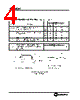
️· AC Performance: AC characteristics (propagation delay, transition time) vary with supply voltage and load capacitance.
In summary, the SL74HC05 is a versatile hex inverter that is well-suited for a variety of digital logic applications, particularly those where open-drain outputs and low power consumption are important considerations.
## SL74HC05 Hex Inverting Buffer Datasheet Summary
This document details the SL74HC05, a hex inverting buffer IC. Here’s a breakdown of the key information:
1. Core Functionality:
️· Type: Hex Inverting Buffer (6 independent inverters)
️· Output Type: Open-drain, requiring pull-up resistors for standard logic levels.
️· Interfaces: Designed to interface with CMOS, NMOS, and TTL logic families.
2. Electrical Characteristics:
️· Supply Voltage (VCC): 2.0V to 6.0V
️· Input Logic Levels:
- VIH (Minimum High Input Voltage): 1.5V (at 2.0V VCC), 3.15V (at 4.5V VCC), 4.2V (at 6.0V VCC)
- VIL (Maximum Low Input Voltage): 0.5V (at 2.0V VCC), 1.35V (at 4.5V VCC), 1.8V (at 6.0V VCC)
️· Output Logic Levels (Low-Level): Typically around 0.1V - 0.4V depending on VCC and load current.
️· Quiescent Supply Current (ICC): 1.0µA (typical)
️· Input Leakage Current (IIN): ±1.0µA
3. AC Performance (Typical - values depend on VCC and load):
️· Propagation Delay (tPLZ, tPZL): As low as 20ns at 6V VCC.
️· Output Transition Time (tTHL): Around 13ns at 6V VCC.
4. Key Features:
️· Open-Drain Outputs: This allows for wired-OR and other custom logic configurations. Requires external pull-up resistors to function as standard logic outputs.
️· Wide Operating Voltage Range: 2.0V to 6.0V provides flexibility in system design.
️· TTL, CMOS, NMOS Compatible: Can be used in mixed-logic environments.
️· Low Power Consumption: Makes it suitable for battery-powered applications.
5. Packages:
️· The datasheet doesn't explicitly mention specific package types, but typical packages for this IC are likely DIP, SOIC, and possibly others.
6. Important Notes:
️· Pull-up Resistors: The open-drain outputs *require* external pull-up resistors to function as standard logic outputs.
️· AC Performance: AC characteristics (propagation delay, transition time) vary with supply voltage and load capacitance.
In summary, the SL74HC05 is a versatile hex inverter that is well-suited for a variety of digital logic applications, particularly those where open-drain outputs and low power consumption are important considerations.
| Part No. | SL74HC05 |
| Manufacturer | SLS |
| Size | 35 Kbytes |
| Pages | 5 pages |
| Description | Hex Inverter with Open-Drain Outputs |
| Lei ha avuto il aiuto da alldatasheet? [ DONATE ] |
Di alldatasheet | Richest di pubblicita | contatti | Privacy Policy | Collegamento alla scheda tecnica | scambio Link | Ricerca produttore All Rights Reserved©Alldatasheet.com |
| Russian : Alldatasheetru.com | Korean : Alldatasheet.co.kr | Spanish : Alldatasheet.es | French : Alldatasheet.fr | Italian : Alldatasheetit.com Portuguese : Alldatasheetpt.com | Polish : Alldatasheet.pl | Vietnamese : Alldatasheet.vn Indian : Alldatasheet.in | Mexican : Alldatasheet.com.mx | British : Alldatasheet.co.uk | New Zealand : Alldatasheet.co.nz |
|
Family Site : ic2ic.com |
icmetro.com |
 Italian ▼
  English
 Chinese
 German
 Japanese
 Russian
 Korean
 Spanish
 French
 Portuguese
 Polish
 Vietnamese
 Indian
 Mexican
 British
 New Zealand