 |
Motore di ricerca datesheet componenti elettronici |
|
|
Motore di ricerca datesheet componenti elettronici |
|
The question interval is too short.
Please try again in a few seconds.

Hello, Please ask a question about LTC3405A Datasheet
# Example questions:
➢ What are the primary differences between forced continuous mode and burst mode operation, and under what circumstances would you choose one over the other?
➢ Describe how the sync/mode pin can be used to both enable burst mode operation and synchronize the internal oscillator to an external clock. what are the implications of each use case?
➢ Explain the function of the track/ss pin. how can it be used to modify the startup behavior of the output voltage, and what are the consequences of leaving it floating?
| Part No. | LTC3405A |
| Manufacturer | LINER |
| Size | 210 Kbytes |
| Pages | 20 pages |
| Description | 2.5A, 10V, Monolithic Synchronous Step-Down Regulator |






1. Overview
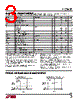
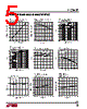
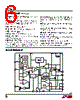
️· Device Type: Monolithic, constant-frequency, current-mode step-down DC/DC converter.
️· Function: Regulates voltage.
️· Package Options: FE/UF and FB (likely referring to different surface mount packages).
2. Pin Functions (Key Pins & Their Roles)
️· SYNC/MODE (Pin 1/4): Selects operating mode (Forced Continuous, Burst Mode). Also allows for external clock synchronization.
️· PGOOD (Pin 2/5): Power Good indicator. Alerts if output voltage is out of spec.
️· RT (Pin 3/6): Frequency Setting. External resistor used to set the switching frequency.
️· ITH (Pin 1/4): Error amplifier compensation point, critical for loop stability.
️· FB (Pin 1/5): Feedback pin - receives the regulated voltage signal.
️· RUN (Pin 1/10): Enables/disables the converter. Can be tied to PVIN for continuous operation.
️· TRACK/SS (Pin 1/11): Used for tracking the output voltage during startup or for external soft-start.
️· SW (Pin 1/12, 13, 16, 17, 18, 19): Switch node - connects to inductor.
️· PVIN (Pin 1/1,2): Power input. Requires decoupling capacitor.
️· INTVCC (Pin 1/16): 5V LDO output.
️· Exposed Pad (Pin 1/21): Signal ground. Crucially, *must* be soldered to the PCB.
3. Operating Modes & Characteristics
️· Forced Continuous Mode:
- Enabled by connecting SYNC/MODE to INTVCC.
- Disables Burst Mode.
- Minimizes switching harmonics but can be less efficient at light loads.
️· Burst Mode Operation:
- Enabled by connecting SYNC/MODE to a voltage between 0.42V and 1V.
- Improves efficiency at light loads by operating the MOSFETs intermittently.
- Minimizes quiescent current.
- Pulse-skipping operation is implemented by connecting the SYNC/MODE pin to ground.
️· Frequency Synchronization:
- Allows synchronizing the internal oscillator to an external clock.
- Frequency range: 300kHz to 3MHz.
4. Key Technical Details & Considerations
️· Switching Frequency: Set by external resistor on the RT pin.
️· Quiescent Current: 75μA in Burst Mode.
️· Current Limit: -2.5A (forced continuous), 0A (Burst Mode).
️· PGOOD Output: Pulled low when output voltage is outside tolerance.
️· Important Note: The exposed pad *must* be soldered to the PCB for proper signal grounding.
1. Overview
️· Device Type: Monolithic, constant-frequency, current-mode step-down DC/DC converter.
️· Function: Regulates voltage.
️· Package Options: FE/UF and FB (likely referring to different surface mount packages).
2. Pin Functions (Key Pins & Their Roles)
️· SYNC/MODE (Pin 1/4): Selects operating mode (Forced Continuous, Burst Mode). Also allows for external clock synchronization.
️· PGOOD (Pin 2/5): Power Good indicator. Alerts if output voltage is out of spec.
️· RT (Pin 3/6): Frequency Setting. External resistor used to set the switching frequency.
️· ITH (Pin 1/4): Error amplifier compensation point, critical for loop stability.
️· FB (Pin 1/5): Feedback pin - receives the regulated voltage signal.
️· RUN (Pin 1/10): Enables/disables the converter. Can be tied to PVIN for continuous operation.
️· TRACK/SS (Pin 1/11): Used for tracking the output voltage during startup or for external soft-start.
️· SW (Pin 1/12, 13, 16, 17, 18, 19): Switch node - connects to inductor.
️· PVIN (Pin 1/1,2): Power input. Requires decoupling capacitor.
️· INTVCC (Pin 1/16): 5V LDO output.
️· Exposed Pad (Pin 1/21): Signal ground. Crucially, *must* be soldered to the PCB.
3. Operating Modes & Characteristics
️· Forced Continuous Mode:
- Enabled by connecting SYNC/MODE to INTVCC.
- Disables Burst Mode.
- Minimizes switching harmonics but can be less efficient at light loads.
️· Burst Mode Operation:
- Enabled by connecting SYNC/MODE to a voltage between 0.42V and 1V.
- Improves efficiency at light loads by operating the MOSFETs intermittently.
- Minimizes quiescent current.
- Pulse-skipping operation is implemented by connecting the SYNC/MODE pin to ground.
️· Frequency Synchronization:
- Allows synchronizing the internal oscillator to an external clock.
- Frequency range: 300kHz to 3MHz.
4. Key Technical Details & Considerations
️· Switching Frequency: Set by external resistor on the RT pin.
️· Quiescent Current: 75μA in Burst Mode.
️· Current Limit: -2.5A (forced continuous), 0A (Burst Mode).
️· PGOOD Output: Pulled low when output voltage is outside tolerance.
️· Important Note: The exposed pad *must* be soldered to the PCB for proper signal grounding.
| Part No. | LTC3405A |
| Manufacturer | LINER |
| Size | 210 Kbytes |
| Pages | 20 pages |
| Description | 2.5A, 10V, Monolithic Synchronous Step-Down Regulator |
| Lei ha avuto il aiuto da alldatasheet? [ DONATE ] |
Di alldatasheet | Richest di pubblicita | contatti | Privacy Policy | Collegamento alla scheda tecnica | scambio Link | Ricerca produttore All Rights Reserved©Alldatasheet.com |
| Russian : Alldatasheetru.com | Korean : Alldatasheet.co.kr | Spanish : Alldatasheet.es | French : Alldatasheet.fr | Italian : Alldatasheetit.com Portuguese : Alldatasheetpt.com | Polish : Alldatasheet.pl | Vietnamese : Alldatasheet.vn Indian : Alldatasheet.in | Mexican : Alldatasheet.com.mx | British : Alldatasheet.co.uk | New Zealand : Alldatasheet.co.nz |
|
Family Site : ic2ic.com |
icmetro.com |
 Italian ▼
  English
 Chinese
 German
 Japanese
 Russian
 Korean
 Spanish
 French
 Portuguese
 Polish
 Vietnamese
 Indian
 Mexican
 British
 New Zealand