 |
Motore di ricerca datesheet componenti elettronici |
|
|
Motore di ricerca datesheet componenti elettronici |
|
The question interval is too short.
Please try again in a few seconds.

Hello, Please ask a question about LT1126_15 Datasheet
# Example questions:
➢ What is the difference in typical supply current per amplifier between the lt1126am and lt1126m?
➢ What is the typical input offset voltage for the lt1126am over the full temperature range?
➢ What is the typical slew rate for the lt1127am with a 2kω load?
| Part No. | LT1126_15 |
| Manufacturer | LINER |
| Size | 280 Kbytes |
| Pages | 12 pages |
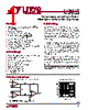
| Description | Dual/Quad Decompensated Low Noise, High Speed Precision Op Amps |


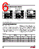
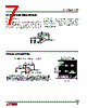


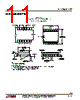
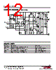

1. Overall Context:
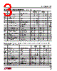
️· Device: LT1126 and LT1127 operational amplifiers.
️· Datasheet Excerpt: This is not the full datasheet; it's a specific section dealing with electrical characteristics.
️· Conditions: Most specifications are given at V<sub>S</sub> = ±15V and a temperature range of 0°C to 70°C unless otherwise specified.
️· "●" Symbol: A crucial element! The "●" symbol indicates that the specification is guaranteed to be valid *over the entire operating temperature range* (likely -55°C to 125°C, although the full datasheet would confirm this). If the "●" is *not* present, the specification applies at the standard test conditions (±15V and 0°C to 70°C).
2. Key Electrical Characteristics & Explanations:
Let's go through the parameters listed (I've included the second set of characteristics for a more complete view):
️· V<sub>OS</sub> (Input Offset Voltage): The difference between the actual output voltage and the ideal output voltage when no input signal is present. A lower value is better (less error).
- LT1126/LT1127 (Standard Conditions): 50µV to 170µV and 55µV to 190µV.
- LT1126/LT1127 (Full Temp Range): 60µV to 250µV and 70µV to 290µV
️· ∆V<sub>OS</sub>/∆T (Input Offset Voltage Drift): How much the input offset voltage changes with temperature. A lower value is better (more stable).
- LT1126/LT1127 (Standard Conditions): 0.3 µV/°C to 1.0 µV/°C.
- LT1126/LT1127 (Full Temp Range): 0.4 µV/°C to 1.5 µV/°C
️· I<sub>OS</sub> (Input Offset Current): The small current that flows into the input terminals due to the input offset voltage circuitry. Lower is better.
- LT1126/LT1127 (Standard Conditions): 18nA to 45nA and 18nA to 55nA.
- LT1126/LT1127 (Full Temp Range): 20nA to 60nA and 20nA to 70nA
️· I<sub>B</sub> (Input Bias Current): The average of the input bias currents at both input terminals. Lower is better.
- LT1126/LT1127 (Standard Conditions): ±18nA to ±55nA.
- LT1126/LT1127 (Full Temp Range): ±20nA to ±70nA
️· V<sub>CM</sub> (Common-Mode Voltage Range): The range of input voltages over which the output voltage remains within specified limits. A wider range is generally desirable.
- LT1126/LT1127 (Standard Conditions): ±11.3V to ±12V.
- LT1126/LT1127 (Full Temp Range): ±11.3V to ±12V
️· CMRR (Common-Mode Rejection Ratio): A measure of the amplifier's ability to reject signals common to both input terminals. A higher value is better.
- LT1126/LT1127 (Standard Conditions): 106 dB to 122 dB
- LT1126/LT1127 (Full Temp Range): 100 dB to 120 dB
️· PSRR (Power Supply Rejection Ratio): A measure of the amplifier's ability to reject variations in the power supply voltage. A higher value is better.
- LT1126/LT1127 (Standard Conditions): 110 dB to 122 dB
- LT1126/LT1127 (Full Temp Range): 104 dB to 120 dB
️· A<sub>VOL</sub> (Voltage Gain): The ratio of the output voltage to the input voltage. Higher is generally better.
- LT1126/LT1127 (Standard Conditions): 3.0 V/µV to 10.0 V/µV, and 1.0 V/µV to 3.0 V/µV
- LT1126/LT1127 (Full Temp Range): 2.0 V/µV to 10.0 V/µV, and 0.7 V/µV to 2.0 V/µV
️· V<sub>OUT</sub> (Maximum Output Voltage Swing): The maximum voltage swing the amplifier can produce.
- LT1126/LT1127 (Standard Conditions): ±12.5 V to ±13.6V
- LT1126/LT1127 (Full Temp Range): ±12.0V to ±13.6V
️· Slew Rate: How quickly the output voltage can change. A higher value is generally better for fast signals.
- LT1126/LT1127 (Standard Conditions): 7.2 V/µs to 10 V/µs
- LT1126/LT1127 (Full Temp Range): 7.0 V/µs to 10 V/µs
️· I<sub>S</sub> (Supply Current): The current drawn from the power supply.
- LT1126/LT1127 (Standard Conditions): 2.8 mA to 3.5 mA
To fully understand the characteristics, you would need the full datasheet.
1. Overall Context:
️· Device: LT1126 and LT1127 operational amplifiers.
️· Datasheet Excerpt: This is not the full datasheet; it's a specific section dealing with electrical characteristics.
️· Conditions: Most specifications are given at V<sub>S</sub> = ±15V and a temperature range of 0°C to 70°C unless otherwise specified.
️· "●" Symbol: A crucial element! The "●" symbol indicates that the specification is guaranteed to be valid *over the entire operating temperature range* (likely -55°C to 125°C, although the full datasheet would confirm this). If the "●" is *not* present, the specification applies at the standard test conditions (±15V and 0°C to 70°C).
2. Key Electrical Characteristics & Explanations:
Let's go through the parameters listed (I've included the second set of characteristics for a more complete view):
️· V<sub>OS</sub> (Input Offset Voltage): The difference between the actual output voltage and the ideal output voltage when no input signal is present. A lower value is better (less error).
- LT1126/LT1127 (Standard Conditions): 50µV to 170µV and 55µV to 190µV.
- LT1126/LT1127 (Full Temp Range): 60µV to 250µV and 70µV to 290µV
️· ∆V<sub>OS</sub>/∆T (Input Offset Voltage Drift): How much the input offset voltage changes with temperature. A lower value is better (more stable).
- LT1126/LT1127 (Standard Conditions): 0.3 µV/°C to 1.0 µV/°C.
- LT1126/LT1127 (Full Temp Range): 0.4 µV/°C to 1.5 µV/°C
️· I<sub>OS</sub> (Input Offset Current): The small current that flows into the input terminals due to the input offset voltage circuitry. Lower is better.
- LT1126/LT1127 (Standard Conditions): 18nA to 45nA and 18nA to 55nA.
- LT1126/LT1127 (Full Temp Range): 20nA to 60nA and 20nA to 70nA
️· I<sub>B</sub> (Input Bias Current): The average of the input bias currents at both input terminals. Lower is better.
- LT1126/LT1127 (Standard Conditions): ±18nA to ±55nA.
- LT1126/LT1127 (Full Temp Range): ±20nA to ±70nA
️· V<sub>CM</sub> (Common-Mode Voltage Range): The range of input voltages over which the output voltage remains within specified limits. A wider range is generally desirable.
- LT1126/LT1127 (Standard Conditions): ±11.3V to ±12V.
- LT1126/LT1127 (Full Temp Range): ±11.3V to ±12V
️· CMRR (Common-Mode Rejection Ratio): A measure of the amplifier's ability to reject signals common to both input terminals. A higher value is better.
- LT1126/LT1127 (Standard Conditions): 106 dB to 122 dB
- LT1126/LT1127 (Full Temp Range): 100 dB to 120 dB
️· PSRR (Power Supply Rejection Ratio): A measure of the amplifier's ability to reject variations in the power supply voltage. A higher value is better.
- LT1126/LT1127 (Standard Conditions): 110 dB to 122 dB
- LT1126/LT1127 (Full Temp Range): 104 dB to 120 dB
️· A<sub>VOL</sub> (Voltage Gain): The ratio of the output voltage to the input voltage. Higher is generally better.
- LT1126/LT1127 (Standard Conditions): 3.0 V/µV to 10.0 V/µV, and 1.0 V/µV to 3.0 V/µV
- LT1126/LT1127 (Full Temp Range): 2.0 V/µV to 10.0 V/µV, and 0.7 V/µV to 2.0 V/µV
️· V<sub>OUT</sub> (Maximum Output Voltage Swing): The maximum voltage swing the amplifier can produce.
- LT1126/LT1127 (Standard Conditions): ±12.5 V to ±13.6V
- LT1126/LT1127 (Full Temp Range): ±12.0V to ±13.6V
️· Slew Rate: How quickly the output voltage can change. A higher value is generally better for fast signals.
- LT1126/LT1127 (Standard Conditions): 7.2 V/µs to 10 V/µs
- LT1126/LT1127 (Full Temp Range): 7.0 V/µs to 10 V/µs
️· I<sub>S</sub> (Supply Current): The current drawn from the power supply.
- LT1126/LT1127 (Standard Conditions): 2.8 mA to 3.5 mA
To fully understand the characteristics, you would need the full datasheet.
| Part No. | LT1126_15 |
| Manufacturer | LINER |
| Size | 280 Kbytes |
| Pages | 12 pages |
| Description | Dual/Quad Decompensated Low Noise, High Speed Precision Op Amps |
| Lei ha avuto il aiuto da alldatasheet? [ DONATE ] |
Di alldatasheet | Richest di pubblicita | contatti | Privacy Policy | Collegamento alla scheda tecnica | scambio Link | Ricerca produttore All Rights Reserved©Alldatasheet.com |
| Russian : Alldatasheetru.com | Korean : Alldatasheet.co.kr | Spanish : Alldatasheet.es | French : Alldatasheet.fr | Italian : Alldatasheetit.com Portuguese : Alldatasheetpt.com | Polish : Alldatasheet.pl | Vietnamese : Alldatasheet.vn Indian : Alldatasheet.in | Mexican : Alldatasheet.com.mx | British : Alldatasheet.co.uk | New Zealand : Alldatasheet.co.nz |
|
Family Site : ic2ic.com |
icmetro.com |
 Italian ▼
  English
 Chinese
 German
 Japanese
 Russian
 Korean
 Spanish
 French
 Portuguese
 Polish
 Vietnamese
 Indian
 Mexican
 British
 New Zealand