 |
Motore di ricerca datesheet componenti elettronici |
|
|
Motore di ricerca datesheet componenti elettronici |
|
The question interval is too short.
Please try again in a few seconds.

Hello, Please ask a question about MCP3201-BIST Datasheet
# Example questions:
➢ What is the primary difference in the test conditions between figure 2-21 (thd vs. input frequency) and figure 2-23 (sinad vs. input frequency)?
➢ How does increasing the input frequency generally affect the total harmonic distortion (thd)?
➢ What are the supply voltage (vdd) and reference voltage (vref) values used for most of the performance characterization data presented in the document?
| Part No. | MCP3201-BIST |
| Manufacturer | MICROCHIP |
| Size | 377 Kbytes |
| Pages | 20 pages |
| Description | 2.7V 12-Bit A/D Converter with SPI Serial Interface |

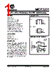
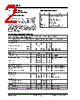
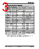
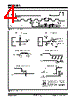


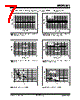



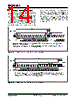

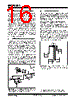


1. Timing Characteristics (from the text - limited detail)
️· Clock Frequency: The text refers to f_CLK being 16 times the sample rate (f_SAMPLE).
️· Sample Rate: f_SAMPLE can vary and is implied to be in the range of 50 kHz to 100 kHz based on figure descriptions.
2. Electrical Characteristics (Extracted from timing references & overall context)
️· Supply Voltage (V<sub>DD</sub>): The ADC can operate with different supply voltages. Specific values mentioned are 2.7V and 5V. Figures show both being used.
️· Reference Voltage (V<sub>REF</sub>): The ADC uses a reference voltage, VREF. Like VDD, it can be either 2.7V or 5V. The ADC's performance is heavily dependent on the stability of VREF.
️· Input Signal Level: The figures show input signal levels ranging from negative to positive values, presented in dB, implying a wide dynamic range for the input signal.
️· Input Signal Frequency: The figures show a broad range of frequency, from 1 kHz to 100 kHz.
3. Performance Characteristics (Based on Figures - Most Detailed Section)
️· Gain Error: (Figure 2-19 & 2-20). Shows the gain error vs. Temperature and Input Frequency. Gain error decreases with increasing temperature.
️· Offset Error: (Figure 2-22 & 2-18). Demonstrates offset error versus temperature and VREF.
️· Signal-to-Noise Ratio (SNR): (Figure 2-21). Increased with input signal frequency.
️· Signal-to-Noise and Distortion (SINAD): (Figures 2-23 & 2-24). Increased with Input Frequency and Signal level.
️· Total Harmonic Distortion (THD): (Figure 2-25). Low THD values were observed across the spectrum.
️· Effective Number of Bits (ENOB): (Figures 2-26 & 2-27). Shows how ENOB changes with VREF and Input frequency.
️· Spurious Free Dynamic Range (SFDR): (Figure 2-28). Indicates the difference between the fundamental signal and the spurious tones.
️· Power Supply Rejection (PSR): (Figure 2-29). Represents the ADC's ability to reject noise on the power supply lines. A higher PSR value indicates better power supply noise rejection.
️· Frequency Spectrum: The diagrams show the spectral content of the ADC output, illustrating the presence of noise and harmonics. Representative spectra for both 10 kHz and 1 kHz input signals are shown, both with the typical and 2.7V voltage.
4. Summary Table (Combined Information)
| Characteristic | Value/Description | Notes |
|---|---|---|
| Supply Voltage (V<sub>DD</sub>) | 2.7V or 5V | Varies depending on application |
| Reference Voltage (V<sub>REF</sub>) | 2.7V or 5V | Must be stable and accurate |
| Input Signal Frequency | 1 kHz to 100 kHz | Wide range, affects SNR and distortion |
| Sample Rate (f<sub>SAMPLE</sub>) | Inferred, likely 50 kHz - 100 kHz | Dependent on application |
| SNR | Increases with frequency | |
| SINAD | Improved with input frequency and Signal Level | |
| ENOB | Varies with VREF and input Frequency | |
| SFDR | Dependent on Input Frequency | |
| PSR | Indicates power supply noise rejection capability |
1. Timing Characteristics (from the text - limited detail)
️· Clock Frequency: The text refers to f_CLK being 16 times the sample rate (f_SAMPLE).
️· Sample Rate: f_SAMPLE can vary and is implied to be in the range of 50 kHz to 100 kHz based on figure descriptions.
2. Electrical Characteristics (Extracted from timing references & overall context)
️· Supply Voltage (V<sub>DD</sub>): The ADC can operate with different supply voltages. Specific values mentioned are 2.7V and 5V. Figures show both being used.
️· Reference Voltage (V<sub>REF</sub>): The ADC uses a reference voltage, VREF. Like VDD, it can be either 2.7V or 5V. The ADC's performance is heavily dependent on the stability of VREF.
️· Input Signal Level: The figures show input signal levels ranging from negative to positive values, presented in dB, implying a wide dynamic range for the input signal.
️· Input Signal Frequency: The figures show a broad range of frequency, from 1 kHz to 100 kHz.
3. Performance Characteristics (Based on Figures - Most Detailed Section)
️· Gain Error: (Figure 2-19 & 2-20). Shows the gain error vs. Temperature and Input Frequency. Gain error decreases with increasing temperature.
️· Offset Error: (Figure 2-22 & 2-18). Demonstrates offset error versus temperature and VREF.
️· Signal-to-Noise Ratio (SNR): (Figure 2-21). Increased with input signal frequency.
️· Signal-to-Noise and Distortion (SINAD): (Figures 2-23 & 2-24). Increased with Input Frequency and Signal level.
️· Total Harmonic Distortion (THD): (Figure 2-25). Low THD values were observed across the spectrum.
️· Effective Number of Bits (ENOB): (Figures 2-26 & 2-27). Shows how ENOB changes with VREF and Input frequency.
️· Spurious Free Dynamic Range (SFDR): (Figure 2-28). Indicates the difference between the fundamental signal and the spurious tones.
️· Power Supply Rejection (PSR): (Figure 2-29). Represents the ADC's ability to reject noise on the power supply lines. A higher PSR value indicates better power supply noise rejection.
️· Frequency Spectrum: The diagrams show the spectral content of the ADC output, illustrating the presence of noise and harmonics. Representative spectra for both 10 kHz and 1 kHz input signals are shown, both with the typical and 2.7V voltage.
4. Summary Table (Combined Information)
| Characteristic | Value/Description | Notes |
|---|---|---|
| Supply Voltage (V<sub>DD</sub>) | 2.7V or 5V | Varies depending on application |
| Reference Voltage (V<sub>REF</sub>) | 2.7V or 5V | Must be stable and accurate |
| Input Signal Frequency | 1 kHz to 100 kHz | Wide range, affects SNR and distortion |
| Sample Rate (f<sub>SAMPLE</sub>) | Inferred, likely 50 kHz - 100 kHz | Dependent on application |
| SNR | Increases with frequency | |
| SINAD | Improved with input frequency and Signal Level | |
| ENOB | Varies with VREF and input Frequency | |
| SFDR | Dependent on Input Frequency | |
| PSR | Indicates power supply noise rejection capability |
| Part No. | MCP3201-BIST |
| Manufacturer | MICROCHIP |
| Size | 377 Kbytes |
| Pages | 20 pages |
| Description | 2.7V 12-Bit A/D Converter with SPI Serial Interface |
| Lei ha avuto il aiuto da alldatasheet? [ DONATE ] |
Di alldatasheet | Richest di pubblicita | contatti | Privacy Policy | Collegamento alla scheda tecnica | scambio Link | Ricerca produttore All Rights Reserved©Alldatasheet.com |
| Russian : Alldatasheetru.com | Korean : Alldatasheet.co.kr | Spanish : Alldatasheet.es | French : Alldatasheet.fr | Italian : Alldatasheetit.com Portuguese : Alldatasheetpt.com | Polish : Alldatasheet.pl | Vietnamese : Alldatasheet.vn Indian : Alldatasheet.in | Mexican : Alldatasheet.com.mx | British : Alldatasheet.co.uk | New Zealand : Alldatasheet.co.nz |
|
Family Site : ic2ic.com |
icmetro.com |
 Italian ▼
  English
 Chinese
 German
 Japanese
 Russian
 Korean
 Spanish
 French
 Portuguese
 Polish
 Vietnamese
 Indian
 Mexican
 British
 New Zealand