 |
Motore di ricerca datesheet componenti elettronici |
|
|
Motore di ricerca datesheet componenti elettronici |
|
The question interval is too short.
Please try again in a few seconds.

Hello, Please ask a question about HDCS1000 Datasheet
# Example questions:
➢ Considering the components listed (pga, adc, row/column decoders), describe in a single sentence how this sensor likely converts light into a digital signal.
➢ What is the primary function of the 'row decoder' and 'column decoder' components within the sensor architecture?
➢ What purpose might these different data output methods serve in a system utilizing this sensor?
| Part No. | HDCS1000 |
| Manufacturer | HP |
| Size | 25 Kbytes |
| Pages | 2 pages |
| Description | Integrated CMOS Image Sensor with Digital Output and Timing Controller |

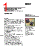

1. Diagram Interpretation (Challenges & Assumptions)
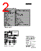
The diagram, as described through text, appears to be a block diagram illustrating the architecture of an image sensor (likely a CMOS image sensor). The text representation is a significant limitation. A true block diagram is visually organized to show connections and relationships. The text format makes it difficult to fully grasp the connections. It *seems* to be a horizontal layout, but that’s not certain.
2. Key Components and Their Functions (as best as possible)
️· Row Decoder: Likely controls the selection of rows within the sensor array.
️· Column Decoder: Likely controls the selection of columns within the sensor array.
️· Row Control, Main Control, Sequencer: These blocks suggest a control system for coordinating the sensor's operations. The 'Sequencer' implies a sequence of operations for imaging.
️· Row Address (Row Addr), Column Address (Column Addr): These are inputs to the decoders, specifying which row and column to activate/read.
️· Register Set: Possibly a collection of registers used to store configuration data or intermediate values.
️· APS ARRAY (Active Pixel Sensor Array): This is the core of the image sensor, where light is converted into electrical signals.
️· PGA (Programmable Gain Amplifier): Amplifies the signal from the APS array.
️· ADC (Analog-to-Digital Converter): Converts the analog signal from the PGA into a digital value.
️· DIN (Data In): Input for data, potentially configuration data or commands.
️· DO (Data Out): Output for image data or status information.
️· SIPO (Serial In, Parallel Out): A serial-to-parallel shift register. Likely used to transfer image data from the sensor array to a processing unit.
️· PISO (Parallel In, Serial Out): A parallel-to-serial shift register. Potentially used to transfer data from a digital processor back to a serial interface.
️· Data, Clock, Control Signals: These are the signals required for data transmission and sensor control.
️· 10-Bit Parallel Data Out: This is the digital image data output.
3. Control Flow (Inferred)
Based on the diagram's likely organization, I infer the following control flow:
1. Addressing: The "Row Address" and "Column Address" signals are input to their respective decoders ("Row Decoder" and "Column Decoder").
2. Pixel Activation & Signal Conversion: The decoders select specific pixels in the "APS ARRAY." Each pixel converts light into an electrical signal.
3. Amplification: The electrical signal is amplified by the "PGA."
4. Digital Conversion: The amplified signal is converted to a digital value by the "ADC."
5. Serial/Parallel Conversion: The digital data is often converted from a serial signal (within the array) to a parallel signal for processing or output. SIPO performs this conversion.
6. Output: The digital data is output either in parallel ("10-Bit Parallel Data Out") or serially.
7. Control: The "Row Control," "Main Control," and "Sequencer" blocks coordinate the entire process, controlling the timing and operation of the other components. The "DIN" signal allows external control.
4. Summary & Potential Limitations
The block diagram represents a typical CMOS image sensor architecture. It highlights the key components involved in light detection, signal processing, and data output. It is likely used for cameras, machine vision systems, or other imaging applications.
Limitations due to Text Representation:
️· Lack of Visual Layout: The most significant limitation is the inability to see the actual layout and connections between blocks. This makes it difficult to fully understand the data flow.
️· Ambiguity: The text format can lead to ambiguity in interpreting the relationships between blocks.
️· Missing Detail: The level of detail in the diagram is likely simplified in the text representation. There are probably more intermediate blocks and connections that are not described.
️· Distortion: The text representation of the diagram is likely to be distorted compared to the original visual representation.
1. Diagram Interpretation (Challenges & Assumptions)
The diagram, as described through text, appears to be a block diagram illustrating the architecture of an image sensor (likely a CMOS image sensor). The text representation is a significant limitation. A true block diagram is visually organized to show connections and relationships. The text format makes it difficult to fully grasp the connections. It *seems* to be a horizontal layout, but that’s not certain.
2. Key Components and Their Functions (as best as possible)
️· Row Decoder: Likely controls the selection of rows within the sensor array.
️· Column Decoder: Likely controls the selection of columns within the sensor array.
️· Row Control, Main Control, Sequencer: These blocks suggest a control system for coordinating the sensor's operations. The 'Sequencer' implies a sequence of operations for imaging.
️· Row Address (Row Addr), Column Address (Column Addr): These are inputs to the decoders, specifying which row and column to activate/read.
️· Register Set: Possibly a collection of registers used to store configuration data or intermediate values.
️· APS ARRAY (Active Pixel Sensor Array): This is the core of the image sensor, where light is converted into electrical signals.
️· PGA (Programmable Gain Amplifier): Amplifies the signal from the APS array.
️· ADC (Analog-to-Digital Converter): Converts the analog signal from the PGA into a digital value.
️· DIN (Data In): Input for data, potentially configuration data or commands.
️· DO (Data Out): Output for image data or status information.
️· SIPO (Serial In, Parallel Out): A serial-to-parallel shift register. Likely used to transfer image data from the sensor array to a processing unit.
️· PISO (Parallel In, Serial Out): A parallel-to-serial shift register. Potentially used to transfer data from a digital processor back to a serial interface.
️· Data, Clock, Control Signals: These are the signals required for data transmission and sensor control.
️· 10-Bit Parallel Data Out: This is the digital image data output.
3. Control Flow (Inferred)
Based on the diagram's likely organization, I infer the following control flow:
1. Addressing: The "Row Address" and "Column Address" signals are input to their respective decoders ("Row Decoder" and "Column Decoder").
2. Pixel Activation & Signal Conversion: The decoders select specific pixels in the "APS ARRAY." Each pixel converts light into an electrical signal.
3. Amplification: The electrical signal is amplified by the "PGA."
4. Digital Conversion: The amplified signal is converted to a digital value by the "ADC."
5. Serial/Parallel Conversion: The digital data is often converted from a serial signal (within the array) to a parallel signal for processing or output. SIPO performs this conversion.
6. Output: The digital data is output either in parallel ("10-Bit Parallel Data Out") or serially.
7. Control: The "Row Control," "Main Control," and "Sequencer" blocks coordinate the entire process, controlling the timing and operation of the other components. The "DIN" signal allows external control.
4. Summary & Potential Limitations
The block diagram represents a typical CMOS image sensor architecture. It highlights the key components involved in light detection, signal processing, and data output. It is likely used for cameras, machine vision systems, or other imaging applications.
Limitations due to Text Representation:
️· Lack of Visual Layout: The most significant limitation is the inability to see the actual layout and connections between blocks. This makes it difficult to fully understand the data flow.
️· Ambiguity: The text format can lead to ambiguity in interpreting the relationships between blocks.
️· Missing Detail: The level of detail in the diagram is likely simplified in the text representation. There are probably more intermediate blocks and connections that are not described.
️· Distortion: The text representation of the diagram is likely to be distorted compared to the original visual representation.
| Part No. | HDCS1000 |
| Manufacturer | HP |
| Size | 25 Kbytes |
| Pages | 2 pages |
| Description | Integrated CMOS Image Sensor with Digital Output and Timing Controller |
| Lei ha avuto il aiuto da alldatasheet? [ DONATE ] |
Di alldatasheet | Richest di pubblicita | contatti | Privacy Policy | Collegamento alla scheda tecnica | scambio Link | Ricerca produttore All Rights Reserved©Alldatasheet.com |
| Russian : Alldatasheetru.com | Korean : Alldatasheet.co.kr | Spanish : Alldatasheet.es | French : Alldatasheet.fr | Italian : Alldatasheetit.com Portuguese : Alldatasheetpt.com | Polish : Alldatasheet.pl | Vietnamese : Alldatasheet.vn Indian : Alldatasheet.in | Mexican : Alldatasheet.com.mx | British : Alldatasheet.co.uk | New Zealand : Alldatasheet.co.nz |
|
Family Site : ic2ic.com |
icmetro.com |
 Italian ▼
  English
 Chinese
 German
 Japanese
 Russian
 Korean
 Spanish
 French
 Portuguese
 Polish
 Vietnamese
 Indian
 Mexican
 British
 New Zealand