 |
Motore di ricerca datesheet componenti elettronici |
|
|
Motore di ricerca datesheet componenti elettronici |
|
The question interval is too short.
Please try again in a few seconds.

Hello, Please ask a question about ADA4355ABCZ Datasheet
# Example questions:
➢ In the provided datasheet excerpts, what does 'ddr' stand for in the context of the lvds output timing diagrams?
➢ What is the minimum aperture delay (ta) for the ada4355 at 25°c?
➢ What is the typical propagation delay (tpd) for the lvds output of the ada4355?
| Part No. | ADA4355ABCZ |
| Manufacturer | AD |
| Size | 1Mb |
| Pages | 45 pages |
| Description | Programmable Transimpedance, Current to Bits Receiver 關Module |


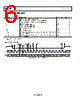
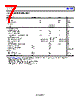
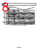
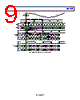
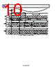
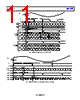
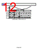

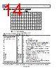
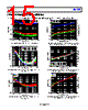
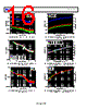

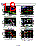
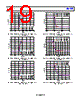
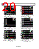

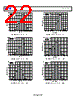
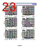
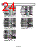
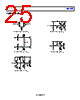
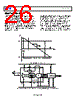
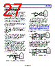

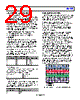
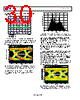
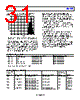

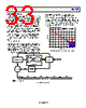
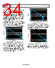
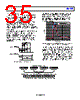
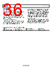
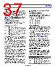
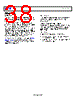



Overall Purpose: The document details the electrical characteristics and timing parameters of the ADA4355, a high-speed Analog-to-Digital Converter (ADC). It focuses on its LVDS (Low-Voltage Differential Signaling) output.
Here's a categorized summary:
1. General Information & Modes:
️· ADC Type: High-Speed ADC
️· Output Signal: LVDS (Low-Voltage Differential Signaling)
️· Data Formats: Supports DDR (Double Data Rate), SDR (Single Data Rate), Bitwise and Bytewise modes.
️· Frame Modes: Includes a 1x frame mode.
️· Data Lanes: Operates with two data lanes.
2. Key Timing Parameters (Values are *critical* - read carefully! The datasheet uses abbreviations. See the end of this summary for common abbreviations):
️· Clock Rate: Ranges from 10 MHz to 1000 MHz.
️· Conversion Rate: Can vary (details in tables).
️· Pulse Width (High/Low - tEH/tEL): Relates to clock pulse duration.
️· Propagation Delay (tPD): Time taken for signal to propagate.
️· Rise/Fall Time (tR/tF): Time for signal transitions.
️· Frame Clock Output Delay (tFCO): Delay of the frame clock output signal.
️· Data Output Delay (tDATA): Delay of the data output signals.
️· Lane Delay (tLD): Delay specific to data lanes.
️· Data Skew (tDATA-MAX - tDATA-MIN): Variation in data arrival times across lanes.
️· Wake-Up Times: Time to transition from standby or power-down states.
️· Pipeline Latency: The number of clock cycles before valid data is available.
️· Aperture Delay (tA): Delay between the ADC's internal sampling clock and the LVDS output.
️· Aperture Uncertainty (Jitter, tJ): Variation in the sampling time (jitter).
️· Out-of-Range Recovery Time: Time needed to recover from an out-of-range condition.
3. Tables of Values (MOST IMPORTANT):
The document presents extensive timing parameters in multiple tables, specifically focused on:
️· Table 6: ADC LVDS Output Timing Diagram: Outlines the timing of DDR/SDR operations in 1x frame mode.
️· Table 3: 12-Bit DDR/SDR, Two-Lane, 1× Frame Mode: Presents a table of parameter values to be used.
️· Table 3: DDR/SDR Operation: Contains numerical values for the key timing parameters listed above.
4. Diagrams:
️· Figure 6: 16-Bit DDR/SDR, Two-Lane, 1× Frame Mode: A visual representation of the DDR/SDR operation.
️· Figure 7: 12-Bit DDR/SDR, Two-Lane, 1× Frame Mode: A visual representation of the 12-bit DDR/SDR operation.
️· Figure 1-5 and 8-11 are also provided, but not explained.
Important Notes from the Document:
️· Application Note: The document refers to Application Note AN-835 for details on ADC testing and evaluation.
️· FR4 Material: Timing characteristics are based on measurements performed on FR4 material.
️· Parameter Definitions: The document uses abbreviations, and many parameters are complex. Consult the datasheet for complete definitions and the context of their use.
Common Abbreviations (likely used in the full datasheet):
️· ADC: Analog-to-Digital Converter
️· LVDS: Low-Voltage Differential Signaling
️· DDR: Double Data Rate
️· SDR: Single Data Rate
️· tPD: Propagation Delay
️· tR: Rise Time
️· tF: Fall Time
️· tJ: Jitter
️· MSB: Most Significant Bit
️· LSB: Least Significant Bit
️· FCO: Frame Clock Output
️· DCO: Data Clock Output
Overall Purpose: The document details the electrical characteristics and timing parameters of the ADA4355, a high-speed Analog-to-Digital Converter (ADC). It focuses on its LVDS (Low-Voltage Differential Signaling) output.
Here's a categorized summary:
1. General Information & Modes:
️· ADC Type: High-Speed ADC
️· Output Signal: LVDS (Low-Voltage Differential Signaling)
️· Data Formats: Supports DDR (Double Data Rate), SDR (Single Data Rate), Bitwise and Bytewise modes.
️· Frame Modes: Includes a 1x frame mode.
️· Data Lanes: Operates with two data lanes.
2. Key Timing Parameters (Values are *critical* - read carefully! The datasheet uses abbreviations. See the end of this summary for common abbreviations):
️· Clock Rate: Ranges from 10 MHz to 1000 MHz.
️· Conversion Rate: Can vary (details in tables).
️· Pulse Width (High/Low - tEH/tEL): Relates to clock pulse duration.
️· Propagation Delay (tPD): Time taken for signal to propagate.
️· Rise/Fall Time (tR/tF): Time for signal transitions.
️· Frame Clock Output Delay (tFCO): Delay of the frame clock output signal.
️· Data Output Delay (tDATA): Delay of the data output signals.
️· Lane Delay (tLD): Delay specific to data lanes.
️· Data Skew (tDATA-MAX - tDATA-MIN): Variation in data arrival times across lanes.
️· Wake-Up Times: Time to transition from standby or power-down states.
️· Pipeline Latency: The number of clock cycles before valid data is available.
️· Aperture Delay (tA): Delay between the ADC's internal sampling clock and the LVDS output.
️· Aperture Uncertainty (Jitter, tJ): Variation in the sampling time (jitter).
️· Out-of-Range Recovery Time: Time needed to recover from an out-of-range condition.
3. Tables of Values (MOST IMPORTANT):
The document presents extensive timing parameters in multiple tables, specifically focused on:
️· Table 6: ADC LVDS Output Timing Diagram: Outlines the timing of DDR/SDR operations in 1x frame mode.
️· Table 3: 12-Bit DDR/SDR, Two-Lane, 1× Frame Mode: Presents a table of parameter values to be used.
️· Table 3: DDR/SDR Operation: Contains numerical values for the key timing parameters listed above.
4. Diagrams:
️· Figure 6: 16-Bit DDR/SDR, Two-Lane, 1× Frame Mode: A visual representation of the DDR/SDR operation.
️· Figure 7: 12-Bit DDR/SDR, Two-Lane, 1× Frame Mode: A visual representation of the 12-bit DDR/SDR operation.
️· Figure 1-5 and 8-11 are also provided, but not explained.
Important Notes from the Document:
️· Application Note: The document refers to Application Note AN-835 for details on ADC testing and evaluation.
️· FR4 Material: Timing characteristics are based on measurements performed on FR4 material.
️· Parameter Definitions: The document uses abbreviations, and many parameters are complex. Consult the datasheet for complete definitions and the context of their use.
Common Abbreviations (likely used in the full datasheet):
️· ADC: Analog-to-Digital Converter
️· LVDS: Low-Voltage Differential Signaling
️· DDR: Double Data Rate
️· SDR: Single Data Rate
️· tPD: Propagation Delay
️· tR: Rise Time
️· tF: Fall Time
️· tJ: Jitter
️· MSB: Most Significant Bit
️· LSB: Least Significant Bit
️· FCO: Frame Clock Output
️· DCO: Data Clock Output
| Part No. | ADA4355ABCZ |
| Manufacturer | AD |
| Size | 1Mb |
| Pages | 45 pages |
| Description | Programmable Transimpedance, Current to Bits Receiver 關Module |
| Lei ha avuto il aiuto da alldatasheet? [ DONATE ] |
Di alldatasheet | Richest di pubblicita | contatti | Privacy Policy | Collegamento alla scheda tecnica | scambio Link | Ricerca produttore All Rights Reserved©Alldatasheet.com |
| Russian : Alldatasheetru.com | Korean : Alldatasheet.co.kr | Spanish : Alldatasheet.es | French : Alldatasheet.fr | Italian : Alldatasheetit.com Portuguese : Alldatasheetpt.com | Polish : Alldatasheet.pl | Vietnamese : Alldatasheet.vn Indian : Alldatasheet.in | Mexican : Alldatasheet.com.mx | British : Alldatasheet.co.uk | New Zealand : Alldatasheet.co.nz |
|
Family Site : ic2ic.com |
icmetro.com |
 Italian ▼
  English
 Chinese
 German
 Japanese
 Russian
 Korean
 Spanish
 French
 Portuguese
 Polish
 Vietnamese
 Indian
 Mexican
 British
 New Zealand