|
Motore di ricerca datesheet componenti elettronici |
|
|
Motore di ricerca datesheet componenti elettronici |
|
ADA4355ABCZ Scheda tecnica(PDF) 6 Page - Analog Devices |
|
|
|||||||||||||||||||||||||||||
ADA4355ABCZ Scheda tecnica(HTML) 6 Page - Analog Devices |
|
|
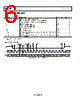
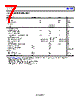
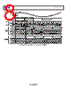
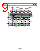
6 / 45 page  ADA4355 Data Sheet Rev. A | Page 6 of 45 ADC SPI TIMING SPECIFICATIONS Table 4. Parameter Description Min Typ Max Unit SPI TIMING REQUIREMENTS See Figure 5, unless otherwise noted tDS Setup time between the data and the rising edge of SCLK 2 ns tDH Hold time between the data and the rising edge of SCLK 2 ns tCLK Period of the SCLK 40 ns tS Setup time between CS and SCLK 2 ns tH Hold time between CS and SCLK 2 ns tHIGH SCLK pulse width high 10 ns tLOW SCLK pulse width low 10 ns tEN_SDIO1 Time required for SDIO to switch from an input to an output relative to the SCLK falling edge 10 ns tDIS_SDIO1 Time required for SDIO to switch from an output to an input relative to the SCLK rising edge 10 ns 1 This parameter is not shown in Figure 5. ADC SPI Timing Diagram DON’T CARE DON’T CARE DON’T CARE DON’T CARE SDIO SCLK CS tS tDH tCLK tDS tH R/W W1 W0 A12 A11 A10 A9 A8 A7 D5 D4 D3 D2 D1 D0 tLOW tHIGH Figure 5. Serial Port Interface Timing Diagram |
|
Link URL |
| Lei ha avuto il aiuto da alldatasheet? [ DONATE ] |
Di alldatasheet | Richest di pubblicita | contatti | Privacy Policy | Collegamento alla scheda tecnica | scambio Link | Ricerca produttore All Rights Reserved©Alldatasheet.com |
| Russian : Alldatasheetru.com | Korean : Alldatasheet.co.kr | Spanish : Alldatasheet.es | French : Alldatasheet.fr | Italian : Alldatasheetit.com Portuguese : Alldatasheetpt.com | Polish : Alldatasheet.pl | Vietnamese : Alldatasheet.vn Indian : Alldatasheet.in | Mexican : Alldatasheet.com.mx | British : Alldatasheet.co.uk | New Zealand : Alldatasheet.co.nz |
|
Family Site : ic2ic.com |
icmetro.com |
 Italian ▼
 English
 Chinese
 German
 Japanese
 Russian
 Korean
 Spanish
 French
 Italian
 Portuguese
 Polish
 Vietnamese
 Indian
 Mexican
 British
 New Zealand