 |
Motore di ricerca datesheet componenti elettronici |
|
|
Motore di ricerca datesheet componenti elettronici |
|
The question interval is too short.
Please try again in a few seconds.

Hello, Please ask a question about ML6440 Datasheet
# Example questions:
➢ Identify all pin numbers that are labeled with 'gnd'.
➢ What digital signal is associated with pin number 39?
➢ List all the pin labels that begin with the letters 'ci'.
| Part No. | ML6440 |
| Manufacturer | MICRO-LINEAR |
| Size | 227 Kbytes |
| Pages | 18 pages |
| Description | Multi-Standard 8-bit Adaptive Digital Input Comb Filter |


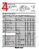


This looks like a pinout diagram for a video processing chip, likely an encoder or scaler. Here's a breakdown of what's represented, categorized for clarity:
1. Chip Identification & Core Function:
️· SmartComb™: This suggests a chip incorporating a comb filter for interlaced video processing (deinterlacing).
️· Video Processing/Encoding/Scaling: The overall function seems to be related to video manipulation - likely combining encoding, scaling, and deinterlacing.
2. Power & Ground Pins:
️· VCC: Positive power supply voltage (likely 3.3V or 5V).
️· AVCC: Analog power supply, possibly needing a separate regulator for clean analog signals.
️· GND: Ground connection (common reference point).
3. Data/Video Input/Output Pins:
️· CI0-CI7: Color Input data pins (likely RGB or YCbCr components).
️· Y0-Y7: Luma (brightness) Input data pins.
️· CO-C7: Color Output data pins.
️· YO-Y7: Luma Output data pins.
️· S CLK: Serial Clock for data transfer.
️· S DATA: Serial Data line.
️· S/P: Serial/Parallel mode selection or output.
4. Control/Configuration Pins:
️· CLK: Clock input for the chip’s internal operations.
️· RST: Reset input - used to initialize the chip.
️· OE: Output Enable – controls whether the output is active.
️· YI0-YI7: Possibly Y component input pins for video.
️· CI0-CI7: color input
️· CO-C7: Color output
5. Timing & Synchronization Pins:
️· Specific timing signals for horizontal and vertical synchronization are likely present, but aren’t explicitly labeled (they would be crucial for video display).
6. Other Notes & Observations:
️· Pin Numbering: The diagram doesn’t include pin numbers. A real datasheet would have this.
️· Data Width: The use of 8 data pins (CI0-CI7, YO-Y7, etc.) suggests a parallel data interface, potentially 8 bits wide.
️· Functionality by Section: There are distinct sections of the pinout: data inputs, data outputs, control, timing, and analog. This suggests a complex, modular design.
To fully understand this pinout, you *absolutely* need the datasheet from the manufacturer. The datasheet will provide:
️· Pin numbers
️· Electrical characteristics (voltage levels, current limits)
️· Timing diagrams
️· Detailed descriptions of each pin’s function and how to use it.
This looks like a pinout diagram for a video processing chip, likely an encoder or scaler. Here's a breakdown of what's represented, categorized for clarity:
1. Chip Identification & Core Function:
️· SmartComb™: This suggests a chip incorporating a comb filter for interlaced video processing (deinterlacing).
️· Video Processing/Encoding/Scaling: The overall function seems to be related to video manipulation - likely combining encoding, scaling, and deinterlacing.
2. Power & Ground Pins:
️· VCC: Positive power supply voltage (likely 3.3V or 5V).
️· AVCC: Analog power supply, possibly needing a separate regulator for clean analog signals.
️· GND: Ground connection (common reference point).
3. Data/Video Input/Output Pins:
️· CI0-CI7: Color Input data pins (likely RGB or YCbCr components).
️· Y0-Y7: Luma (brightness) Input data pins.
️· CO-C7: Color Output data pins.
️· YO-Y7: Luma Output data pins.
️· S CLK: Serial Clock for data transfer.
️· S DATA: Serial Data line.
️· S/P: Serial/Parallel mode selection or output.
4. Control/Configuration Pins:
️· CLK: Clock input for the chip’s internal operations.
️· RST: Reset input - used to initialize the chip.
️· OE: Output Enable – controls whether the output is active.
️· YI0-YI7: Possibly Y component input pins for video.
️· CI0-CI7: color input
️· CO-C7: Color output
5. Timing & Synchronization Pins:
️· Specific timing signals for horizontal and vertical synchronization are likely present, but aren’t explicitly labeled (they would be crucial for video display).
6. Other Notes & Observations:
️· Pin Numbering: The diagram doesn’t include pin numbers. A real datasheet would have this.
️· Data Width: The use of 8 data pins (CI0-CI7, YO-Y7, etc.) suggests a parallel data interface, potentially 8 bits wide.
️· Functionality by Section: There are distinct sections of the pinout: data inputs, data outputs, control, timing, and analog. This suggests a complex, modular design.
To fully understand this pinout, you *absolutely* need the datasheet from the manufacturer. The datasheet will provide:
️· Pin numbers
️· Electrical characteristics (voltage levels, current limits)
️· Timing diagrams
️· Detailed descriptions of each pin’s function and how to use it.
| Part No. | ML6440 |
| Manufacturer | MICRO-LINEAR |
| Size | 227 Kbytes |
| Pages | 18 pages |
| Description | Multi-Standard 8-bit Adaptive Digital Input Comb Filter |
| Lei ha avuto il aiuto da alldatasheet? [ DONATE ] |
Di alldatasheet | Richest di pubblicita | contatti | Privacy Policy | Collegamento alla scheda tecnica | scambio Link | Ricerca produttore All Rights Reserved©Alldatasheet.com |
| Russian : Alldatasheetru.com | Korean : Alldatasheet.co.kr | Spanish : Alldatasheet.es | French : Alldatasheet.fr | Italian : Alldatasheetit.com Portuguese : Alldatasheetpt.com | Polish : Alldatasheet.pl | Vietnamese : Alldatasheet.vn Indian : Alldatasheet.in | Mexican : Alldatasheet.com.mx | British : Alldatasheet.co.uk | New Zealand : Alldatasheet.co.nz |
|
Family Site : ic2ic.com |
icmetro.com |
 Italian ▼
  English
 Chinese
 German
 Japanese
 Russian
 Korean
 Spanish
 French
 Portuguese
 Polish
 Vietnamese
 Indian
 Mexican
 British
 New Zealand