|
Motore di ricerca datesheet componenti elettronici |
|
|
Motore di ricerca datesheet componenti elettronici |
|
AD830JRZ-R7 Scheda tecnica(PDF) 15 Page - Analog Devices |
|
|
|||||||||||||||||||||||||||||
AD830JRZ-R7 Scheda tecnica(HTML) 15 Page - Analog Devices |
|
|
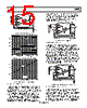
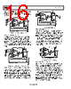
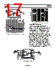
15 / 20 page  Data Sheet AD830 Rev. D | Page 15 of 20 VP VOUT AD830 1 2 3 4 8 7 6 5 A = 1 C VICM VIN VOCM VOUT = (VIN – VICM) + VOCM GM GM Figure 35. General Single-Supply Connection DIFFERENTIAL INPUTVOLTAGE (VPEAK) 16 0 0 2.0 0.4 1.2 1.6 0.8 8 4 12 VP = +30V VP = +15V VP = +10V TO GND 20 24 28 30 Figure 36. Input Common-Mode Range for Single Supply SUPPLY VOLTAGE (V) 16 0 30 10 14 18 22 26 8 4 12 20 24 28 TO VP TO GND Figure 37. Output Swing Limit for Single Supply Differential Line Receiver The AD830 is specifically designed to perform as a differential line receiver. The circuit in Figure 38 shows how simple it is to configure the AD830 for this function. The signal from System A is received differentially relative to the common of System A, and that voltage is exactly reproduced relative to the common in System B. The common-mode rejection versus frequency, shown in Figure 6, is excellent, typically 100 dB at low frequencies. The high input impedance permits the AD830 to operate as a bridging amplifier across low impedance terminations with negligible loading. The differential gain and phase specifications are very good, as shown in Figure 12 for 500 Ω and Figure 15 for 150 Ω. The input and output common should be separated to achieve the full CMR performance of the AD830 as a differential amplifier. However, a common return path is necessary between System A and System B. COMMON IN SYSTEM A VN AD830 1 2 3 4 8 7 6 5 A = 1 GM GM C VCM ZCM COMMON IN SYSTEM B VP VOUT 0.1µF 0.1µF INPUT SIGNAL V1 V2 VOUT = V1 – V2 Figure 38. Differential Line Receiver Wide Range Level Shifter The wide common-mode range and accuracy of the AD830 allows easy level shifting of differential signals referred to an input common-mode voltage to any new voltage defined at the output. The inputs may be referenced to levels as high as 10 V at the inputs with a ±2 V swing around 10 V. In the circuit in Figure 39, the output voltage, VOUT, is defined by the simple equation shown below. The excellent linearity and low distortion are preserved over the full input and output common-mode range. The voltage sources need not be of low impedance, since the high input resistance and modest input bias current of the AD830 V-to-I converters permit the use of resistive voltage dividers as reference voltages. GM VP VOUT INPUT COMMON VN 0.1µF AD830 1 2 3 4 8 7 6 5 A = 1 C 0.1µF INPUT SIGNAL V1 V2 OUTPUT COMMON V3 VOUT = V1 – V2 + V3 GM Figure 39. Differential Amplification with Level Shifting Difference Amplifier with Gain > 1 The AD830 can provide instrumentation amplifier style and differential amplification at gains greater than 1. The input signal is connected differentially and the gain is set via feedback resistors, as shown in Figure 40. The gain is G = (R2 + R1)/R2. The AD830 can provide either inverting or noninverting differential amplification. The polarity of the gain is established by the polarity of the connection at the input. Feedback resistor, R2, should generally be R2 ≤ 1 kΩ to maintain closed-loop |
|
|
Link URL |
| Lei ha avuto il aiuto da alldatasheet? [ DONATE ] |
Di alldatasheet | Richest di pubblicita | contatti | Privacy Policy | Collegamento alla scheda tecnica | scambio Link | Ricerca produttore All Rights Reserved©Alldatasheet.com |
| Russian : Alldatasheetru.com | Korean : Alldatasheet.co.kr | Spanish : Alldatasheet.es | French : Alldatasheet.fr | Italian : Alldatasheetit.com Portuguese : Alldatasheetpt.com | Polish : Alldatasheet.pl | Vietnamese : Alldatasheet.vn Indian : Alldatasheet.in | Mexican : Alldatasheet.com.mx | British : Alldatasheet.co.uk | New Zealand : Alldatasheet.co.nz |
|
Family Site : ic2ic.com |
icmetro.com |
 Italian ▼
 English
 Chinese
 German
 Japanese
 Russian
 Korean
 Spanish
 French
 Italian
 Portuguese
 Polish
 Vietnamese
 Indian
 Mexican
 British
 New Zealand