|
Motore di ricerca datesheet componenti elettronici |
|
|
Motore di ricerca datesheet componenti elettronici |
|
ADR370ART-R2 Scheda tecnica(PDF) 6 Page - Analog Devices |
|
|
|||||||||||||||||||||||||||||
ADR370ART-R2 Scheda tecnica(HTML) 6 Page - Analog Devices |
|
|
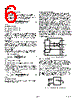
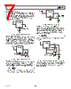
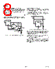
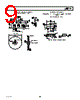
6 / 12 page  REV. A –6– ADR370 PARAMETER DEFINITIONS Temperature Coefficient Temperature coefficient is the change of output voltage with respect to operating temperature changes, normalized by the output voltage at 25 °C. This parameter is expressed in ppm/°C and can be determined with the following equation TCV ppm C VT VT VC T T O OO O ° = ()− () ° ()×− () × 21 21 6 25 10 (1) where: VO (25 °C) = V O at 25 °C. VO (T1) = VO at Temperature 1. VO (T2) = VO at Temperature 2. Line Regulation Line regulation is the change in output voltage due to a specified change in input voltage. This parameter accounts for the effects of self-heating. Line regulation is expressed in either percent per volt, parts-per-million per volt, or microvolts per volt change in input voltage. Load Regulation Load regulation is the change in output voltage due to a specified change in load current. This parameter accounts for the effects of self-heating. Load regulation is expressed in either microvolts per milliampere, parts-per-million per milliampere, or ohms of dc output resistance. Long Term Stability Long term stability is the typical shift of output voltage at 25 °C on a sample of parts subjected to a test of 1,000 hours at 25 °C. ∆ ∆ VV t V t V ppm Vt Vt Vt OO O O OO O = ()− () [] = () − () () × 01 01 0 6 10 (2) where: VO (T1) = VO at 25 °C at time 0. VO (T2) = VO at 25 °C after 1,000 hours operation at 25°C. Thermal Hysteresis Thermal hysteresis is defined as the change of output voltage after the device is cycled through temperature from +25 °C to –40°C to +125 °C and back to +25°C. This is a typical value from a sample of parts put through such a cycle. VV C V V ppm VC V VC O HYS O O TC O HYS OO TC O __ _ _ =° ()− [] = ° ()− ° () × 25 25 25 10 6 (3) where: VO (25 °C) = VO at 25°C. VO_TC = VO at 25 °C after temperature cycle at +25°C to –40°C to +125 °C and back to +25°C. THEORY OF OPERATION The ADR370 uses the band-gap concept to produce a stable, low temperature coefficient voltage reference suitable for high accuracy data acquisition components and systems. This device makes use of underlying temperature characteristics of a silicon transistor’s base-emitter voltage (VBE) in the forward biased operating region. Under this condition, all such transistors have a –2 mV/ °C temperature coefficient (TC) and a V BE that, when extrapolated to absolute zero, 0 K, (with collector current pro- portional to absolute temperature) approximates the silicon band-gap voltage. By summing a voltage that has an equal and opposite temperature coefficient of 2 mV/ °C with a V BE of a forward biased transistor, an almost zero TC reference can be developed. The simplified circuit diagram in Figure 1 shows how a compensating voltage, V1, is achieved by driving two transistors at different current densities and amplifying the resultant VBE difference ( ∆V BE, which has a positive TC). The sum (VBG) of VBE and V1 is then buffered and amplified to produce a stable reference voltage of 2.048 V at the output. VIN VOUT GND VDS R5 R6 R4 R3 R2 R1 V1 Figure 1. Simplified Schematic Applying the ADR370 In order to achieve the specified performance, two external components should be used in conjunction with the ADR370, a 4.7 µF capacitor and a 1 µF capacitor should be applied to the input and output, respectively. Figure 2 shows the ADR370 with both the input and output capacitors attached. For further transient response optimization, an additional 0.1 µF capacitor in parallel with the 4.7 µF input capacitor can be used. A 1 µF output capacitor will provide stable performance for all loading conditions. The ADR370 can, however, operate under low (–100 µA < I OUT < +100 µA) current conditions with just a 0.2 µF output capacitor and a 1 µF input capacitor. CIN VIN ADR370 GND 4.7 F COUT VOUT 1 F Figure 2. Typical Connection Diagram |
|
|
Link URL |
| Lei ha avuto il aiuto da alldatasheet? [ DONATE ] |
Di alldatasheet | Richest di pubblicita | contatti | Privacy Policy | Collegamento alla scheda tecnica | scambio Link | Ricerca produttore All Rights Reserved©Alldatasheet.com |
| Russian : Alldatasheetru.com | Korean : Alldatasheet.co.kr | Spanish : Alldatasheet.es | French : Alldatasheet.fr | Italian : Alldatasheetit.com Portuguese : Alldatasheetpt.com | Polish : Alldatasheet.pl | Vietnamese : Alldatasheet.vn Indian : Alldatasheet.in | Mexican : Alldatasheet.com.mx | British : Alldatasheet.co.uk | New Zealand : Alldatasheet.co.nz |
|
Family Site : ic2ic.com |
icmetro.com |
 Italian ▼
 English
 Chinese
 German
 Japanese
 Russian
 Korean
 Spanish
 French
 Italian
 Portuguese
 Polish
 Vietnamese
 Indian
 Mexican
 British
 New Zealand