|
Motore di ricerca datesheet componenti elettronici |
|
|
Motore di ricerca datesheet componenti elettronici |
|
HMC1126ACEZ-R7 Scheda tecnica(PDF) 16 Page - Analog Devices |
|
|
|||||||||||||||||||||||||||||
HMC1126ACEZ-R7 Scheda tecnica(HTML) 16 Page - Analog Devices |
|
|
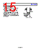
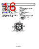
16 / 21 page  HMC1126ACEZ Data Sheet Rev. 0 | Page 16 of 21 APPLICATIONS INFORMATION Figure 57 shows the basic connections for operating the HMC1126ACEZ. Because the RFIN and RFOUT pins are internally ac-coupled, no external ac coupling is required. Because VDD, VGG1, and VGG2 are internally decoupled, no external components are required on these pins. Figure 57 shows the configuration used to characterize and qualify the device. See the HMC1126-EVALZ user guide for information on using the evaluation board. POWER-UP AND POWER-DOWN SEQUENCING To avoid damaging the device, careful attention must be paid to the power-up and power-down sequencing of the RF input, the gate bias voltages, and the drain bias voltage. Power-Up The following power-up sequencing is recommended: 1. Connect GND to ground. 2. Set VGG1 to −2 V. 3. Set VDD to 5 V. 4. Set VGG2 to 1 V. 5. Increase VGG1 to achieve an IDQ = 85 mA. 6. Apply the RF signal. Power-Down The following power-down sequencing is recommended: 1. Turn off the RF signal. 2. Decrease VGG1 to −2 V to achieve an IDQ = 0 mA. 3. Decrease VGG2 to 0 V. 4. Decrease VDD to 0 V. 5. Increase VGG1 to 0 V. 2 1 3 4 5 6 18 17 16 15 14 13 GND RFIN GND GND RFOUT VGG1 (–2V TO 0V) VGG2 (1V) VDD (5V) GND Figure 57. Basic Connections |
|
|
Link URL |
| Lei ha avuto il aiuto da alldatasheet? [ DONATE ] |
Di alldatasheet | Richest di pubblicita | contatti | Privacy Policy | Collegamento alla scheda tecnica | scambio Link | Ricerca produttore All Rights Reserved©Alldatasheet.com |
| Russian : Alldatasheetru.com | Korean : Alldatasheet.co.kr | Spanish : Alldatasheet.es | French : Alldatasheet.fr | Italian : Alldatasheetit.com Portuguese : Alldatasheetpt.com | Polish : Alldatasheet.pl | Vietnamese : Alldatasheet.vn Indian : Alldatasheet.in | Mexican : Alldatasheet.com.mx | British : Alldatasheet.co.uk | New Zealand : Alldatasheet.co.nz |
|
Family Site : ic2ic.com |
icmetro.com |
 Italian ▼
 English
 Chinese
 German
 Japanese
 Russian
 Korean
 Spanish
 French
 Italian
 Portuguese
 Polish
 Vietnamese
 Indian
 Mexican
 British
 New Zealand