4
SP8690/SP8691
DUT
450
0.1
µ
OUTPUTS TO
SAMPLING
SCOPE
VEE
5
9
8
2
1
16
10n
10n
33
33
20
INPUT FROM
GENERATOR
INPUT
MONITOR
450
0.1
µ
2·4k
0.1
µ
VCC
560
11
312
Q4
Q4
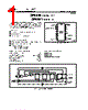
Fig. 8 Test circuit for dynamic measurements
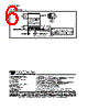
Fig. 9 Typical application showing interfacing.
OPERATING NOTES
1. The clock inputs can be single or differentially driven. The
clock input is biased internally and is coupled to the signal
source with a suitable capacitor. The input signal path is
completed by an input reference decoupling capacitor which
is connected to ground.
2. In the absence of a signal the device will self-oscillate. If
this is undesirable, it may be prevented by connecting a
68k
Ω resistor from the input to V
EE i.e., from pin 1 or pin 16
to pin 12. This reduces the input sensitiviy by approximately
100mV.
3. The circuit will operate down to DC but slew rate must be
better than 100V/
µs.
4. The Q4 and Q4 outputs are compatible with ECLII but can
be interfaced to ECL10K as shown in Fig. 9.
5. The PE inputs are ECLIII/10K compatible and include
internal 10k
Ωpulldown resistors. Unused inputs can therefore
be left open circuit.
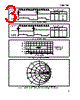
6. The input impedance of the SP8690/1 varies as a function
of frequency. See Fig. 7.
7. The TTL/CMOS output is a free collector and the high
state output voltage will depend on the supply that the
collector load is taken to. This should not exceed 12V.
8. The rise/fall time of the open collector output waveform is
directly proportional to load capacitance and load resistor
value. Therefore, load capacitance should be minimised
and the load resistor kept to a minimum consistent with
system power requirements. In the test configuration of Fig.
8 the output rise time is approximately 10ns and the fall time
DIVIDE BY
10/11 (SP8690)
8/9 (SP8691)
9
8
3k
3k
10k
10k
23
8
1
16
5
BIAS
ECL10K
OUTPUT
3k
68k
10n
TTL
CONTROL INPUT
(SEE TRUTH TABLES,
FIGS. 4 AND 5)
10n
3k
91
O/C
CLOCK
INPUT
11
TTL
OUTPUT
3·6k
1·5k
560
VCC
VEE


 Italian ▼
 English
 Chinese
 German
 Japanese
 Russian
 Korean
 Spanish
 French
 Italian
 Portuguese
 Polish
 Vietnamese
 Indian
 Mexican
 British
 New Zealand