|
Motore di ricerca datesheet componenti elettronici |
|
|
Motore di ricerca datesheet componenti elettronici |
|
74HC393D Scheda tecnica(PDF) 4 Page - Burr-Brown (TI) |
|
|
|
|||||||||||||||||||||||||||||
74HC393D Scheda tecnica(HTML) 4 Page - Burr-Brown (TI) |
|
|
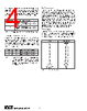
4 / 13 page  4 ® DEM-ADS7843E/45E DUT. Refer to the ADS7843 or ADS7845 data sheet for the proper restrictions on this clock. Alternatively, a clock oscil- lator that is installed in Y1 can be used as the master clock. The signal from this device is either divided by 10 or divided by 20 per JP5. The settings from JP5 are listed in Table VI. JUMPER SETTING RESULTING CONFIGURATION A Y1 Frequency divided by 10. In conjunction with JP6 = B, this frequency becomes DCLK for the DUT. B Y1 frequency divided by 20. In conjunction with JP6 = B, this frequency becomes DCLK for the DUT. TABLE VI. Jumper Settings for Using Y1 as Master Clock. Clocks per Conversion Control Once DCLK is set (per clock control instructions) the conversion cycle of the DUT can be configured to either take 16 or 24 clock cycles. The jumper configuration for these two modes of operation are shown in Table VII. Addition- ally, the timing diagram of these two modes of operation are shown in Figures 2 and 3. JP7 JP8 RESULTING CONFIGURATION A B 24 DCLK cycles per conversion B A 16 DCLK cycles per conversion TABLE VII. The Digital Support Circuitry Can be Operated in a 16 Clocks per Conversion or a 24 Clocks per Conversion with the Jumper Settings De- scribed in the Table. Refer to Figures 2 and 3 for specific timing. DIN Programming The DIN input (DUT, pin 14) receives an 8-bit serial input data stream which programs the ADS7843 or ADS7845 X or Y input channel, mode and power-down options. This serial stream can be programmed with JP3. JP3 is essentailly an 8- bit parallel configuration which is processed by a parallel-to- serial converter (U8) and then transmitted to the DUT at the appropriate time. Even when a position on JP3 is jumper top configured, digital gates can over drive their settings. Con- sequently, these lines are also connected to the digital breadboard area, which gives the user more flexibility in terms of programming this serial command byte. Parallel Output The combination of U13 and U14 converts the digital output of the DUT into a parallel word. This parallel word appears on the connector J3. A DVALID trigger is also provided on J3. Refer to Table VIII for the J3 connector configuration. J3 PIN DESCRIPTION 1 DVALID 11 LSB 13 LSB + 1 15 LSB + 2 17 LSB + 3 19 LSB + 4 21 LSB + 5 23 LSB + 6 25 LSB + 7 27 LSB + 8 29 LSB + 9 31 LSB + 10 33 MSB 3, 5, 7, 9 Digital LOW 35 through 50 Open All Even Pins GND TABLE VIII. J3 Configuration. |
|
|
Link URL |
| Lei ha avuto il aiuto da alldatasheet? [ DONATE ] |
Di alldatasheet | Richest di pubblicita | contatti | Privacy Policy | Collegamento alla scheda tecnica | scambio Link | Ricerca produttore All Rights Reserved©Alldatasheet.com |
| Russian : Alldatasheetru.com | Korean : Alldatasheet.co.kr | Spanish : Alldatasheet.es | French : Alldatasheet.fr | Italian : Alldatasheetit.com Portuguese : Alldatasheetpt.com | Polish : Alldatasheet.pl | Vietnamese : Alldatasheet.vn Indian : Alldatasheet.in | Mexican : Alldatasheet.com.mx | British : Alldatasheet.co.uk | New Zealand : Alldatasheet.co.nz |
|
Family Site : ic2ic.com |
icmetro.com |
 Italian ▼
 English
 Chinese
 German
 Japanese
 Russian
 Korean
 Spanish
 French
 Italian
 Portuguese
 Polish
 Vietnamese
 Indian
 Mexican
 British
 New Zealand