|
Motore di ricerca datesheet componenti elettronici |
|
|
Motore di ricerca datesheet componenti elettronici |
|
AT45DB021B-RU Scheda tecnica(PDF) 17 Page - ATMEL Corporation |
|
|
|||||||||||||||||||||||||||||
AT45DB021B-RU Scheda tecnica(HTML) 17 Page - ATMEL Corporation |
|
|
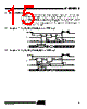
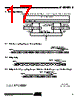
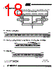
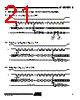
17 / 32 page  17 1937J–DFLSH–9/05 AT45DB021B 10. Write Operations The following block diagram and waveforms illustrate the various write sequences available. 10.1 Main Memory Page Program through Buffers 10.2 Buffer Write 10.3 Buffer to Main Memory Page Program (Data from Buffer Programmed into Flash Page) FLASH MEMORY ARRAY PAGE (256 BYTES) BUFFER 2 (256 BYTES) BUFFER 1 (256 BYTES) I/O INTERFACE SI BUFFER 1 TO PAGE PROGRAM PAGE PROGRAM THROUGH BUFFER 2 BUFFER 2 TO PAGE PROGRAM PAGE PROGRAM THROUGH BUFFER 1 BUFFER 1 WRITE BUFFER 2 WRITE SI CMD n n+1 Last Byte · Completes writing into selected buffer · Starts self-timed erase/program operation CS rrrr r, PA9-7 PA6-0, BFA8 BFA7-0 SI CMD X X···X, BFA8 BFA7-0 n n+1 Last Byte · Completes writing into selected buffer CS SI CMD rrrr r, PA9-7 PA6-0, X CS Starts self-timed erase/program operation X Each transition represents 8 bits and 8 clock cycles n = 1st byte read n+1 = 2nd byte read |
|
Link URL |
| Lei ha avuto il aiuto da alldatasheet? [ DONATE ] |
Di alldatasheet | Richest di pubblicita | contatti | Privacy Policy | Collegamento alla scheda tecnica | scambio Link | Ricerca produttore All Rights Reserved©Alldatasheet.com |
| Russian : Alldatasheetru.com | Korean : Alldatasheet.co.kr | Spanish : Alldatasheet.es | French : Alldatasheet.fr | Italian : Alldatasheetit.com Portuguese : Alldatasheetpt.com | Polish : Alldatasheet.pl | Vietnamese : Alldatasheet.vn Indian : Alldatasheet.in | Mexican : Alldatasheet.com.mx | British : Alldatasheet.co.uk | New Zealand : Alldatasheet.co.nz |
|
Family Site : ic2ic.com |
icmetro.com |
 Italian ▼
 English
 Chinese
 German
 Japanese
 Russian
 Korean
 Spanish
 French
 Italian
 Portuguese
 Polish
 Vietnamese
 Indian
 Mexican
 British
 New Zealand