|
Motore di ricerca datesheet componenti elettronici |
|
|
Motore di ricerca datesheet componenti elettronici |
|
ADIN2111CCPZ-R7 Scheda tecnica(PDF) 12 Page - Analog Devices |
|
|
|||||||||||||||||||||||||||||
ADIN2111CCPZ-R7 Scheda tecnica(HTML) 12 Page - Analog Devices |
|
|
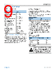
12 / 129 page  Data Sheet ADIN2111 PIN CONFIGURATION AND FUNCTION DESCRIPTIONS analog.com Rev. A | 12 of 129 Table 8. Pin Function Descriptions (Continued) Pin No. Mnemonic1 PU/PD2 Description 48 P2_LED_1/P2_TX2P4_EN PD General-Purpose, Programmable LED Indicator 1 for Port 2 (P2_LED_1). The LED can be active high or active low. The default configuration is P2_LED_1 disabled. See the Status LEDs section. Port 2 Transmit Level Amplitude Hardware Configuration Pin Signal (P2_TX2P4_EN). Set high for 1.0 V p-p transmit amplitude only. Set low to support both 1.0 V p-p and 2.4 V p-p transmit amplitude. See Table 20. The default configuration is 1.0 V p-p and 2.4 V. This pin is provided with an internal pull-down resistor. LDO and Reference Decoupling 9 CEXT_2 N/A Port 2 PHY External Decoupling for Band Gap Voltage Reference. Connect a 0.1 μF capacitor to ground as close as possible to this pin. Do not use this pin as a voltage source for an external circuit. 10 CEXT_3 N/A Port 2 PHY External Decoupling for LDO Circuit. Connect a 1 μF capacitor to ground as close as possible to this pin. Do not use this pin as a voltage source for an external circuit. 32 CEXT_6 N/A Port 1 PHY External Decoupling for Band Gap Voltage Reference. Connect a 0.1 μF capacitor to ground as close as possible to this pin. Do not use this pin as a voltage source for an external circuit. 33 CEXT_7 N/A Port 1 PHY External Decoupling for LDO Circuit. Connect a 1.0 μF capacitor to ground as close as possible to this pin. Do not use this pin as a voltage source for an external circuit. Power and Ground Pins 6, 7, 29, 30 AVDD_H N/A Main Analog Supply Voltage for the Various Analog Circuits in the Device. This supply rail can be supplied by 1.8 V to 3.3 V depending on the transmit level configuration. If AVDD_H is 3.3 V, both the 1.0 V p-p and 2.4 V p-p transmit operating modes are supported. If AVDD_H is 1.8 V, only the 1.0 V p-p transmit operating mode is supported. Connect 0.1 μF and 0.01 μF capacitors to GND as close as possible to this pin. 12, 13, 35, 36 AVDD_L N/A Main Analog Supply Voltage for the Internal LDO Circuits. This supply rail can be supplied by 1.8 V to 3.3 V. AVDD_L can be connected directly to the AVDD_H rail in long reach applications or alternatively to the VDDIO rail when the device is configured with dual supplies for lower power consumption. Connect 0.1 μF and 0.01 μF capacitors to GND as close as possible to this pin. 18, 46 VDDIO N/A 3.3 V, 2.5 V, or 1.8 V Digital Power for the SPI Host Interface. Connect 0.1 μF and 0.01 μF capacitors to GND as close as possible to the pin. 14 DLDO2_1P1 N/A Output from the Internal 1.1 V LDO Circuit 2. When using the internal LDO, connect this pin directly to the DVDD_1P1 pin. Connect a 0.68 μF capacitor to ground as close as possible to this pin. 15 DVDD2_1P1 N/A Input for PHY 1.1 V DVDD Supply Rail 2. When using the internal LDO regulator, connect this pin directly to the DLDO2_1P1 pin. Alternatively, an external 1.1 V rail can be provided to the DVDD_1P1 pin for greater power efficiency. Connect a 0.1 µF to ground as close as possible to this pin. 37 DLDO1_1P1 N/A Output from the 1.1 V LDO Circuit 1. When using the internal LDO, connect this pin directly to the DVDD_1P1 pin 38. Connect a 0.68 μF capacitor to ground as close as possible to this pin. 38 DVDD1_1P1 N/A Input for PHY 1.1 V DVDD Supply Rail 1. When using the internal LDO regulator, connect this pin directly to the DLDO1_1P1 pin. Alternatively, an external 1.1 V rail can be provided to the DVDD_1P1 pin for greater power efficiency. Connect a 0.1 µF to ground as close as possible to this pin. EP (GND) N/A Exposed Pad (Ground). The LFCSP has an exposed pad that must be connected to GND for electrical reasons and soldered to a metal plate on the PCB for mechanical reasons. A 4 × 4 array of thermal vias beneath the exposed GND pad is also recommended. Other Pins 2, 3, 8, 11, 25, 26, 31, 34 DNC N/A Do Not Connect. These pins must be left open circuit. 1 Where a pin is shared between a functional signal and a hardware configuration pin signal, the hardware configuration pin signal is listed last. 2 PU is pull-up, and PD is pull-down. The internal pull-up or pull-down resistor is predefined and nonconfigurable. N/A means not applicable. |
|
Link URL |
| Lei ha avuto il aiuto da alldatasheet? [ DONATE ] |
Di alldatasheet | Richest di pubblicita | contatti | Privacy Policy | Collegamento alla scheda tecnica | scambio Link | Ricerca produttore All Rights Reserved©Alldatasheet.com |
| Russian : Alldatasheetru.com | Korean : Alldatasheet.co.kr | Spanish : Alldatasheet.es | French : Alldatasheet.fr | Italian : Alldatasheetit.com Portuguese : Alldatasheetpt.com | Polish : Alldatasheet.pl | Vietnamese : Alldatasheet.vn Indian : Alldatasheet.in | Mexican : Alldatasheet.com.mx | British : Alldatasheet.co.uk | New Zealand : Alldatasheet.co.nz |
|
Family Site : ic2ic.com |
icmetro.com |
 Italian ▼
 English
 Chinese
 German
 Japanese
 Russian
 Korean
 Spanish
 French
 Italian
 Portuguese
 Polish
 Vietnamese
 Indian
 Mexican
 British
 New Zealand