|
Motore di ricerca datesheet componenti elettronici |
|
|
Motore di ricerca datesheet componenti elettronici |
|
KB3440EDD Scheda tecnica(PDF) 6 Page - Kingbor Technology Co |
|
|
|||||||||||||||||||||||||||||
KB3440EDD Scheda tecnica(HTML) 6 Page - Kingbor Technology Co |
|
|
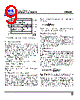
6 / 20 page  6 RT (Pin 1): Timing Resistor to Program the Oscillator Frequency. The programming frequency range is 300kHz to 2MHz. f R Hz OSC T = 61010 • MODE/SYNC (Pin 2): MODE/SYNC = External CLK : Syn- chronization of the internal oscillator. A clock frequency of twice the desired switching frequency and with a pulse width between 100ns and 2 µs is applied. The oscillator free running frequency is set slower than the desired synchronized switching frequency to guarantee sync. The oscillator RT component value required is given by: R f T SW = 81010 • where fSW = desired synchronized switching frequency. SW1 (Pin 3): Switch Pin Where the Internal Switches A and B are Connected. Connect inductor from SW1 to SW2. An optional Schottky diode can be connected from SW1 to ground. Minimize trace length to keep EMI down. SW2 (Pin 4): Switch Pin Where the Internal Switches C and D are Connected. For applications with output volt- ages over 4.3V, a Schottky diode is required from SW2 to VOUT to ensure the SW pin does not exhibit excess voltage. GND (Pin 5): Signal and Power Ground for the IC. VOUT (Pin 6): Output of the Synchronous Rectifier. A filter capacitor is placed from VOUT to GND. VIN (Pin 7): Input Supply Pin. Internal VCC for the IC. A ceramic bypass capacitor as close to the VIN pin and GND (Pin 5) is required. SHDN/SS (Pin 8): Combined Soft-Start and Shutdown. Grounding this pin shuts down the IC. Tie to >1.5V to enable the IC and > 2.5V to ensure the error amp is not clamped from soft-start. An RC from the shutdown com- mand signal to this pin will provide a soft-start function by limiting the rise time of the VC pin. FB (Pin 9): Feedback Pin. Connect resistor divider tap here. The output voltage can be adjusted from 2.5V to 5.5V. The feedback reference voltage is typically 1.22V. VC (Pin 10): Error Amp Output. A frequency compensation network is connected from this pin to the FB pin to compensate the loop. See the section “Compensating the Feedback Loop” for guidelines. Exposed Pad (Pin 11, DFN Package Only): Ground. This pin must be soldered to the PCB and electrically connected to ground. kB3440 Kingbor Technology Co.,Ltd TEL:(86)0755-26508846 FAX:(86)0755-26509052 PIN FUNCTIONS |
|
|
Link URL |
| Lei ha avuto il aiuto da alldatasheet? [ DONATE ] |
Di alldatasheet | Richest di pubblicita | contatti | Privacy Policy | Collegamento alla scheda tecnica | scambio Link | Ricerca produttore All Rights Reserved©Alldatasheet.com |
| Russian : Alldatasheetru.com | Korean : Alldatasheet.co.kr | Spanish : Alldatasheet.es | French : Alldatasheet.fr | Italian : Alldatasheetit.com Portuguese : Alldatasheetpt.com | Polish : Alldatasheet.pl | Vietnamese : Alldatasheet.vn Indian : Alldatasheet.in | Mexican : Alldatasheet.com.mx | British : Alldatasheet.co.uk | New Zealand : Alldatasheet.co.nz |
|
Family Site : ic2ic.com |
icmetro.com |
 Italian ▼
 English
 Chinese
 German
 Japanese
 Russian
 Korean
 Spanish
 French
 Italian
 Portuguese
 Polish
 Vietnamese
 Indian
 Mexican
 British
 New Zealand