|
Motore di ricerca datesheet componenti elettronici |
|
|
Motore di ricerca datesheet componenti elettronici |
|
HIP2103-4DEMO2Z Scheda tecnica(PDF) 26 Page - Renesas Technology Corp |
|
|
|||||||||||||||||||||||||||||
HIP2103-4DEMO2Z Scheda tecnica(HTML) 26 Page - Renesas Technology Corp |
|
|
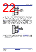
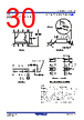
26 / 31 page  HIP2103, HIP2104 8. General EPAD Heatsinking Considerations FN8276 Rev.2.0 Page 26 of 30 Feb 25, 2021 8. General EPAD Heatsinking Considerations The EPAD of the HIP2103 and HIP2104 is electrically connected to VSS through the IC substrate. The EPAD has two main functions: • To provide a quiet signal ground • To provide heat sinking for the IC The EPAD must be connected to a ground plane and switching currents from the driven FETs should not pass through the ground plane under the IC. Figure 28 is a PCB layout example of how to use vias to remove heat from the IC through the EPAD. For maximum heatsinking, it is recommended that a ground plane, connected to the EPAD, is added to both sides of the PCB. A via array within the area of the EPAD conducts heat from the EPAD to the GND plane on the bottom layer. The number of vias and the size of the GND planes required for adequate heatsinking is determined by the power dissipated by the HIP2103 and HIP2104, the air flow, and the maximum temperature of the air around the IC. Note that a separate plane is added under the high side drive circuits and is connected to HS. In a manner similar to the ground plane, the HS plane provides the lowest possible parasitic inductance for the HO/HS gate drive current loop. See AN1899 “HIP2103 and HIP2104 3-phase, Full, or Half Bridge Motor Driver” for an example of PCB layout of a real application. VDD EPAD GND Plane Component Layer HI LI LS HB HO HS LO EPAD GND Plane Bottom Layer VDD HI LI LS HB HO HS LO This plane is connected to HS and is under all high side driver circuits Figure 28. Typical PCB Pattern for Thermal Vias |
|
Link URL |
| Lei ha avuto il aiuto da alldatasheet? [ DONATE ] |
Di alldatasheet | Richest di pubblicita | contatti | Privacy Policy | Collegamento alla scheda tecnica | scambio Link | Ricerca produttore All Rights Reserved©Alldatasheet.com |
| Russian : Alldatasheetru.com | Korean : Alldatasheet.co.kr | Spanish : Alldatasheet.es | French : Alldatasheet.fr | Italian : Alldatasheetit.com Portuguese : Alldatasheetpt.com | Polish : Alldatasheet.pl | Vietnamese : Alldatasheet.vn Indian : Alldatasheet.in | Mexican : Alldatasheet.com.mx | British : Alldatasheet.co.uk | New Zealand : Alldatasheet.co.nz |
|
Family Site : ic2ic.com |
icmetro.com |
 Italian ▼
 English
 Chinese
 German
 Japanese
 Russian
 Korean
 Spanish
 French
 Italian
 Portuguese
 Polish
 Vietnamese
 Indian
 Mexican
 British
 New Zealand