|
Motore di ricerca datesheet componenti elettronici |
|
|
Motore di ricerca datesheet componenti elettronici |
|
CM6800AGIP Scheda tecnica(PDF) 10 Page - Champion Microelectronic Corp. |
|
|
|||||||||||||||||||||||||||||
CM6800AGIP Scheda tecnica(HTML) 10 Page - Champion Microelectronic Corp. |
|
|
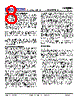
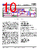
10 / 18 page  CM6800A LOW START-UP CURRENT PFC/PWM CONTROLLER COMBO 2006/10/11 Rev. 1.3 Champion Microelectronic Corporation Page 10 OSCILLATOR 3 ISENSE 7 RAMP1 GAIN MODULATOR 4 VRMS 2 IAC 18 VFB 12 PFC OUT 7.5V REFERENCE 1 IEAO 13 VCC 16 VEAO 14 VREF 0.5V 0.3V -1V VCC 2.5V 17.9V VCC GND 2.75V MNPFC GMi + - . + - VCC OVP MPPFC S R Q Q GMv + - . 3.5K + - PFC ILIMIT 3.5K PFC OVP + - . + - S R Q Q CLK LOW POWER DETECT PFC CMP POWER FACTOR CORRECTOR TRI-FAULT Figure 1. PFC Section Block Diagram Error Amplifier Compensation The PWM loading of the PFC can be modeled as a negative resistor; an increase in input voltage to the PWM causes a decrease in the input current. This response dictates the proper compensation of the two transconductance error amplifiers. Figure 2 shows the types of compensation networks most commonly used for the voltage and current error amplifiers, along with their respective return points. The current loop compensation is returned to VREF to produce a soft-start characteristic on the PFC: as the reference voltage comes up from zero volts, it creates a differentiated voltage on IEAO which prevents the PFC from immediately demanding a full duty cycle on its boost converter. PFC Voltage Loop There are two major concerns when compensating the voltage loop error amplifier, VEAO; stability and transient response. Optimizing interaction between transient response and stability requires that the error amplifier’s open-loop crossover frequency should be 1/2 that of the line frequency, or 23Hz for a 47Hz line (lowest anticipated international power frequency). The gain vs. input voltage of the CM6800A’s voltage error amplifier, VEAO has a specially shaped non-linearity such that under steady-state operating conditions the transconductance of the error amplifier is at a local minimum. Rapid perturbation in line or load conditions will cause the input to the voltage error amplifier (VFB) to deviate from its 2.5V (nominal) value. If this happens, the transconductance of the voltage error amplifier will increase significantly, as shown in the Typical Performance Characteristics. This raises the gain-bandwidth product of the voltage loop, resulting in a much more rapid voltage loop response to such perturbations than would occur with a conventional linear gain characteristics. The Voltage Loop Gain (S) CV V DC EAO 2 OUTDC IN FB EAO OUT FB EAO OUT Z * GM * C * S * V * V V 5 . 2 * P V V * V V * V V Δ ≈ Δ Δ Δ Δ Δ Δ = ZCV: Compensation Net Work for the Voltage Loop GMv: Transconductance of VEAO PIN: Average PFC Input Power VOUTDC: PFC Boost Output Voltage; typical designed value is 380V. CDC: PFC Boost Output Capacitor PFC Current Loop The current amplifier, IEAO compensation is similar to that of the voltage error amplifier, VEAO with exception of the choice of crossover frequency. The crossover frequency of the current amplifier should be at least 10 times that of the voltage amplifier, to prevent interaction with the voltage loop. It should also be limited to less than 1/6th that of the switching frequency, e.g. 16.7kHz for a 100kHz switching frequency. The Current Loop Gain (S) CI I S OUTDC SENSE EAO EAO OFF OFF ISENSE Z * GM * V 5 . 2 * L * S R * V I I * I D * D V ≈ Δ Δ Δ Δ Δ Δ = |
|
|
Link URL |
| Lei ha avuto il aiuto da alldatasheet? [ DONATE ] |
Di alldatasheet | Richest di pubblicita | contatti | Privacy Policy | Collegamento alla scheda tecnica | scambio Link | Ricerca produttore All Rights Reserved©Alldatasheet.com |
| Russian : Alldatasheetru.com | Korean : Alldatasheet.co.kr | Spanish : Alldatasheet.es | French : Alldatasheet.fr | Italian : Alldatasheetit.com Portuguese : Alldatasheetpt.com | Polish : Alldatasheet.pl | Vietnamese : Alldatasheet.vn Indian : Alldatasheet.in | Mexican : Alldatasheet.com.mx | British : Alldatasheet.co.uk | New Zealand : Alldatasheet.co.nz |
|
Family Site : ic2ic.com |
icmetro.com |
 Italian ▼
 English
 Chinese
 German
 Japanese
 Russian
 Korean
 Spanish
 French
 Italian
 Portuguese
 Polish
 Vietnamese
 Indian
 Mexican
 British
 New Zealand