|
Motore di ricerca datesheet componenti elettronici |
|
|
Motore di ricerca datesheet componenti elettronici |
|
ASM3P622S00AG-08-SR Scheda tecnica(PDF) 5 Page - PulseCore Semiconductor |
|
|
|||||||||||||||||||||||||||||
ASM3P622S00AG-08-SR Scheda tecnica(HTML) 5 Page - PulseCore Semiconductor |
|
|
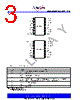
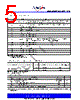
5 / 16 page  May 2007 ASM3P622S00A/B/J/E/K rev 0.4 Low Frequency Timing-Safe™ Peak EMI Reduction IC 5 of 16 Notice: The information in this document is subject to change without notice. Pin Description for ASM3P622S00K Pin # Pin Name Description 1 XIN/CLKIN Crystal connection or external reference frequency input. This pin has dual functions. It can be connected either to an external crystal or an external reference clock. 2 XOUT Crystal connection. If using an external reference, this pin must be left unconnected. 3 CLKOUT1 1 Buffered clock output 4 VDD 3.3V supply 5 SS% 2 Spread Spectrum Selection 6 GND Ground 7 CLKOUT2 1 Buffered clock output 8 CLKOUT3 1 Buffered clock output 9 SSON 2 Spread Spectrum enable and disable option. When SSON is HIGH, the spread spectrum is enabled and when LOW, it turns off the spread spectrum. 10 CLKOUT4 1 Buffered clock output 11 CLKOUT5 1 Buffered clock output 12 GND Ground 13 VDD 3.3V supply 14 CLKOUT6 1 Buffered clock output 15 CLKOUT7 1 Buffered clock output 16 CLKOUT 1 Buffered clock output Notes: 1. Weak pull-down on all outputs 2. Weak pull-up on these Inputs 3. Buffered clock outputs are Timing-Safe™ Spread Spectrum Control and Input-Output Skew Table Device Input Frequency SS % Deviation Input-Output Skew(±TSKEW) 0 ±0.25 % 0.063 ASM3P622S00A/B/J/E/K 12MHz 1 ±0.50 % 0.125 Note: TSKEW is measured in units of the Clock Period Absolute Maximum Ratings Symbol Parameter Rating Unit VDD Voltage on any pin with respect to Ground -0.5 to +4.6 V TSTG Storage temperature -65 to +125 °C Ts Max. Soldering Temperature (10 sec) 260 °C TJ Junction Temperature 150 °C TDV Static Discharge Voltage (As per JEDEC STD22- A114-B) 2 KV Note: These are stress ratings only and are not implied for functional use. Exposure to absolute maximum ratings for prolonged periods of time may affect device reliability. |
|
|
Link URL |
| Lei ha avuto il aiuto da alldatasheet? [ DONATE ] |
Di alldatasheet | Richest di pubblicita | contatti | Privacy Policy | Collegamento alla scheda tecnica | scambio Link | Ricerca produttore All Rights Reserved©Alldatasheet.com |
| Russian : Alldatasheetru.com | Korean : Alldatasheet.co.kr | Spanish : Alldatasheet.es | French : Alldatasheet.fr | Italian : Alldatasheetit.com Portuguese : Alldatasheetpt.com | Polish : Alldatasheet.pl | Vietnamese : Alldatasheet.vn Indian : Alldatasheet.in | Mexican : Alldatasheet.com.mx | British : Alldatasheet.co.uk | New Zealand : Alldatasheet.co.nz |
|
Family Site : ic2ic.com |
icmetro.com |
 Italian ▼
 English
 Chinese
 German
 Japanese
 Russian
 Korean
 Spanish
 French
 Italian
 Portuguese
 Polish
 Vietnamese
 Indian
 Mexican
 British
 New Zealand