|
Motore di ricerca datesheet componenti elettronici |
|
|
Motore di ricerca datesheet componenti elettronici |
|
AS8SLC128K32P-25L/IT Scheda tecnica(PDF) 5 Page - Austin Semiconductor |
|
|
|||||||||||||||||||||||||||||
AS8SLC128K32P-25L/IT Scheda tecnica(HTML) 5 Page - Austin Semiconductor |
|
|
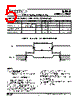
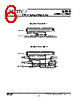
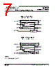
5 / 10 page  SRAM SRAM SRAM SRAM SRAM AS8SLC128K32 AustinSemiconductor,Inc.reservestherighttochangeproductsorspecificationswithoutnotice. 5 AS8SLC128K32 Rev. 0.6 06/05 Austin Semiconductor, Inc. LOW V CC DATA RETENTION WAVEFORM LOW POWER CHARACTERISTICS (L Version Only) 12345678901234567 12345678901234567 12345678901234567 12345678901234567 12345678901234567 12345678901234567 12345678901234567 12345678901234567 12345 12345 12345 12345 12345 12345 12345 12345 1234567 1234567 1234567 1234567 1234567 1234567 1234567 1234567 12345678901234567 12345678901234567 12345678901234567 12345678901234567 12345678901234567 12345678901234567 12345678901234567 12345678901234567 12345 12345 12345 12345 12345 12345 12345 12345 1234567 1234567 1234567 1234567 1234567 1234567 1234567 1234567 DATA RETENTION MODE 4.5V 4.5V V DR > 2V V DR tCDR tR V CC CS\ 1-4 DESCRIPTION SYMBOL MIN MAX UNITS NOTES VCC for Retention Data VDR 2V VCC = 2V ICCDR 24 mA VCC = 3V ICCDR 32 mA Chip Deselect to Data Retention Time tCDR 0ns 4 Operation Recovery Time tR 20 ms 4, 11 Data Retention Current All Inputs @ Vcc + 0.2V or Vss + 0.2V, CS\ = Vcc + 0.2V CONDITIONS t HZCS, is less than tLZCS, and tHZWE is less than tLZWE. 8. WE\ is HIGH for READ cycle. 9. Device is continuously selected. Chip selects and output enable are held in their active state. 10. Address valid prior to or coincident with latest oc- curring chip enable. 11. t RC= READ cycle time. 12. Chip enable (CS\) and write enable (WE\) can initiate and terminate a WRITE cycle. 13. I CC is for full 32 bit mode. NOTES 1. All voltages referenced to V SS (GND). 2. Worst case address switching. 3. ICC is dependent on output loading and cycle rates. The specified value applies with the outputs 4. This parameter guaranteed but not tested. 5. Test conditions as specified with output loading as shown in Fig. 1 & 2 unless otherwise noted. 6. t HZCS, tHZOE and tHZWE are specified with CL= 5pF as in Fig. 2. Transition is measured +/- 200 mV typical from steady state voltage, allowing for actual tester RC time constant. 7. At any given temperature and voltage condition, RC(MIN) unloaded, and f= HZ. t 1 |
|
|
Link URL |
| Lei ha avuto il aiuto da alldatasheet? [ DONATE ] |
Di alldatasheet | Richest di pubblicita | contatti | Privacy Policy | Collegamento alla scheda tecnica | scambio Link | Ricerca produttore All Rights Reserved©Alldatasheet.com |
| Russian : Alldatasheetru.com | Korean : Alldatasheet.co.kr | Spanish : Alldatasheet.es | French : Alldatasheet.fr | Italian : Alldatasheetit.com Portuguese : Alldatasheetpt.com | Polish : Alldatasheet.pl | Vietnamese : Alldatasheet.vn Indian : Alldatasheet.in | Mexican : Alldatasheet.com.mx | British : Alldatasheet.co.uk | New Zealand : Alldatasheet.co.nz |
|
Family Site : ic2ic.com |
icmetro.com |
 Italian ▼
 English
 Chinese
 German
 Japanese
 Russian
 Korean
 Spanish
 French
 Italian
 Portuguese
 Polish
 Vietnamese
 Indian
 Mexican
 British
 New Zealand