|
Motore di ricerca datesheet componenti elettronici |
|
|
Motore di ricerca datesheet componenti elettronici |
|
ZXFV4089 Scheda tecnica(PDF) 7 Page - Diodes Incorporated |
|
|
|||||||||||||||||||||||||||||
ZXFV4089 Scheda tecnica(HTML) 7 Page - Diodes Incorporated |
|
|
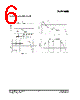
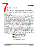
7 / 12 page  ZXFV4089 Issue 4 - December 2008 7 www.zetex.com © Diodes Incorporated 2008 www.diodes.com ZXFV4089 detailed operating notes Introduction This device provides an uncommitted video feed-back amplifier together with a sample-hold system to allow restoration or level-shifting of the input waveform to a controlled DC level. The connection diagram, Figure 1 shows a typical video signal application. No output termination is shown in the diagram, but if desired the output can drive a 75 cable via a 75 series terminating resistor. Amplifier configuration The main amplifier uses current feedback in a non-inverting configuration. Two external resistors are required to set the gain. An external reference, VREF, normally ground, is used to set the new DC level of the video signal. The input video signal is applied via an external input AC coupling capacitor, which is used to store a DC control level when the sample-hold switch is open. Typically an external sampling pulse (active low) is applied to the HOLD input. During this pulse, the sample-hold switch is closed. This completes the DC feedback loop and the stored level is driven towards a new value. At the end of the sampling pulse, the switch opens again and the DC level remains close to the new established value until the next sample pulse. The sample-hold charging current is limited to 300µA. Therefore the convergence towards the steady condition is typically slow, but after several HOLD pulse cycles, the DC level settles closely to the Reference level at the VREF input. The sample-hold loop contains the video amplifier within its path, and also includes an additional sample-hold sense amplifier that compares VREF with the output voltage using an internal low- pass filter. In the high state, the switch is open and the average DC level remains fixed apart from a small drift due to the input bias current of the amplifier and switch leakage (see below). DC restoration The HOLD input is a TTL compatible signal that is buffered and controls the sample-hold switch. A logic LOW state closes the switch and so enables the feedback control loop to set the output level equal to VREF (usually ground). The level of DC shift is maintained when the logic control returns to the HIGH state and the switch opens. In this way the whole waveform is conditionally level shifted, or 'restored' to the new DC level. Figure 2 shows the response of the circuit to a stationary or very slowly varying waveform with an initial voltage offset difference between V+ and VREF, applied to the input coupling capacitor, when the HOLD input is cycled with a repetitive pulse waveform. When the HOLD input is at a logic LOW level, the signal input V+ is driven towards VREF. After a number of cycles, the waveform settles to the DC stabilised value. The waveform is unaffected during the logic HIGH interval of the HOLD input. Figure 2 Response to slow input signal |
|
|
Link URL |
| Lei ha avuto il aiuto da alldatasheet? [ DONATE ] |
Di alldatasheet | Richest di pubblicita | contatti | Privacy Policy | Collegamento alla scheda tecnica | scambio Link | Ricerca produttore All Rights Reserved©Alldatasheet.com |
| Russian : Alldatasheetru.com | Korean : Alldatasheet.co.kr | Spanish : Alldatasheet.es | French : Alldatasheet.fr | Italian : Alldatasheetit.com Portuguese : Alldatasheetpt.com | Polish : Alldatasheet.pl | Vietnamese : Alldatasheet.vn Indian : Alldatasheet.in | Mexican : Alldatasheet.com.mx | British : Alldatasheet.co.uk | New Zealand : Alldatasheet.co.nz |
|
Family Site : ic2ic.com |
icmetro.com |
 Italian ▼
 English
 Chinese
 German
 Japanese
 Russian
 Korean
 Spanish
 French
 Italian
 Portuguese
 Polish
 Vietnamese
 Indian
 Mexican
 British
 New Zealand