|
Motore di ricerca datesheet componenti elettronici |
|
|
Motore di ricerca datesheet componenti elettronici |
|
ADP2164ACPZ-R7 Scheda tecnica(PDF) 16 Page - Analog Devices |
|
|
|||||||||||||||||||||||||||||
ADP2164ACPZ-R7 Scheda tecnica(HTML) 16 Page - Analog Devices |
|
|
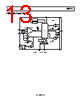
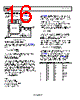
16 / 20 page  ADP2164 Data Sheet Rev. 0 | Page 16 of 20 APPLICATIONS INFORMATION The typical application circuit for the ADP2164 is shown in Figure 38. ADP2164ACPZ CIN 47µF X5R 10V COUT1 47µF X5R 6.3V COUT2 100µF X5R 6.3V VOUT 1.2V 4A VIN 3.3V SYNC TRK FB RT SW SW SW PVIN GND PGND PGND PGND L 0.8µH RTOP 10kΩ RBOT 10kΩ L: MSS1048-801NL COILCRAFT CIN: C3225X5R1A476M TDK COUT1: C3225X5R0J476M TDK COUT2: C3225X5R0J107M TDK 12 11 10 9 4 3 2 1 56 7 8 PGOOD C1 0.1µF EN R1 10Ω R2 10kΩ PVIN 16 15 VIN 14 13 Figure 38. Typical Application Circuit OUTPUT VOLTAGE SELECTION The output voltage of the adjustable version of the ADP2164 is set by an external resistive voltage divider using the following equation: ⎟⎟ ⎠ ⎞ ⎜⎜ ⎝ ⎛ + × = BOT TOP OUT R R V 1 6 . 0 To limit output voltage accuracy degradation due to FB bias current (0.1 μA maximum) to less than 0.5% (maximum), ensure that RBOT is less than 30 kΩ. INDUCTOR SELECTION The inductor value is determined by the operating frequency, input voltage, output voltage, and ripple current. A small inductor value provides larger inductor current ripple and fast transient response but degrades efficiency; a large inductor value provides small inductor current ripple and good efficiency but slows transient response. For a reasonable trade-off between transient response and efficiency, the inductor current ripple, ΔIL, is typically set to one-third the maximum load current. The inductor value is calculated using the following equation: ( ) S L OUT IN f I D V V L × Δ × − = where: VIN is the input voltage. VOUT is the output voltage. ΔIL is the inductor current ripple. fS is the switching frequency. D is the duty cycle (VOUT/VIN). The ADP2164 uses slope compensation in the current control loop to prevent subharmonic oscillations when the duty cycle is larger than 50%. The internal slope compensation limits the minimum inductor value. The negative current limit (−1.3 A) also limits the minimum inductor value. The inductor current ripple (ΔIL) calculated by the selected inductor should not exceed 2.6 A. The peak inductor current should be kept below the peak current limit threshold and is calculated using the following equation: 2 L O PEAK I I I Δ + = Ensure that the rms current of the selected inductor is greater than the maximum load current and that its saturation current is greater than the peak current limit of the converter. OUTPUT CAPACITOR SELECTION The output capacitor value is determined by the output voltage ripple, load step transient, and loop stability. The output ripple is determined by the ESR and the capacitance. ⎟ ⎟ ⎠ ⎞ ⎜ ⎜ ⎝ ⎛ × × + × Δ = Δ S OUT L OUT f C ESR I V 8 1 The load step transient response depends on the inductor, the output capacitor, and the current control loop. The ADP2164 has integrated loop compensation for simple power design. Table 5 and Table 6 show the recommended values for inductors and capacitors for the ADP2164 based on the input and output voltages for the part. X5R or X7R dielectric ceramic capacitors are highly recommended. Table 5. Recommended L and COUT Values at fS = 1.2 MHz VIN (V) VOUT (V) L (μH) COUT (μF) 3.3 1.0 0.8 100 + 100 3.3 1.2 0.8 100 + 47 3.3 1.5 1 100 + 47 3.3 1.8 1 100 3.3 2.5 1 47 5 1.0 0.8 100 + 100 5 1.2 0.8 100 + 47 5 1.5 1 100 + 47 5 1.8 1 100 5 2.5 1 47 5 3.3 1 47 |
|
|
Link URL |
| Lei ha avuto il aiuto da alldatasheet? [ DONATE ] |
Di alldatasheet | Richest di pubblicita | contatti | Privacy Policy | Collegamento alla scheda tecnica | scambio Link | Ricerca produttore All Rights Reserved©Alldatasheet.com |
| Russian : Alldatasheetru.com | Korean : Alldatasheet.co.kr | Spanish : Alldatasheet.es | French : Alldatasheet.fr | Italian : Alldatasheetit.com Portuguese : Alldatasheetpt.com | Polish : Alldatasheet.pl | Vietnamese : Alldatasheet.vn Indian : Alldatasheet.in | Mexican : Alldatasheet.com.mx | British : Alldatasheet.co.uk | New Zealand : Alldatasheet.co.nz |
|
Family Site : ic2ic.com |
icmetro.com |
 Italian ▼
 English
 Chinese
 German
 Japanese
 Russian
 Korean
 Spanish
 French
 Italian
 Portuguese
 Polish
 Vietnamese
 Indian
 Mexican
 British
 New Zealand