|
Motore di ricerca datesheet componenti elettronici |
|
|
Motore di ricerca datesheet componenti elettronici |
|
ICM7712 Scheda tecnica(PDF) 6 Page - IC MICROSYSTEMS |
|
|
|||||||||||||||||||||||||||||
ICM7712 Scheda tecnica(HTML) 6 Page - IC MICROSYSTEMS |
|
|
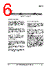
6 / 9 page  ICM7712 Rev A1.5 ICmic reserves the right to change specifications without prior notice 6 FUNCTION C3 C2 C1 C0 DATA D FUNCTION 0 0 0 0 (D11~D0) Input loaded into DAC, VO updated Table 1. Serial Interface Input Word DETAILED DESCRIPTION The ICM7712 is a 12-bit voltage output DAC. This device has a 16-bit input shift register and the DAC has a double buffered digital input. This DAC has a guaranteed monotonic behavior and the operating supply range is from 0.9v to 1.32v. Reference Input The reference input accepts positive DC and AC signals. The voltage at REFIN sets the full-scale output voltage of the DAC. To determine the output voltage for any code, use the following equation. VOUT = VREF x (D / (2 n)) Where D is the numeric value of DAC’s decimal input code, VREF is the reference voltage and n is number of bits, i.e. 12 for ICM7712. Output Buffer Amplifier This amplifier has a wide output voltage swing. The actual swing of the output amplifier will be limited by offset error and gain error. See the Applications Information Section for a more detailed discussion. The output amplifier can drive a load of 2.0 K Ω to VDD or GND in parallel with a 500 pF load capacitance. The output amplifier has a full-scale typical settling time of 2 µs and it dissipates about 500 µA with a 1.2V supply voltage. Serial Interface and Input Logic This DAC uses a standard 3-wire connection compatible with SPI/QSP and Micro wire interfaces. Data is always loaded in 16-bit words which consist of 4 control bits (MSBs) followed by 12 bits (see Figure 3). Serial Data Input SDI (Serial Data Input) pin is the data input pin for the DAC. Data is clocked in on the falling edge of SCK which has a Schmitt trigger internally to allow for noise immunity on the SCK pin. This specially eases the use for opto- coupled interfaces. The Chip Select pin which is the 3rd pin of 8 Lead TSSOP package is active low. This pin frames the input data for synchronous loading and must be low when data is being clocked into the part. There is an onboard counter on the clock input and after the 16th clock pulse the data is automatically transferred to a 16-bit input latch and the 4 bit control word (C3~C0) is then decoded and the appropriate command is performed depending on the control word (see Table 1). Chip Select pin must be pulled high (level-triggered) and back low for the next data word to be loaded in. This pin also disables the SCK pin internally when pulled high. |
|
|
Link URL |
| Lei ha avuto il aiuto da alldatasheet? [ DONATE ] |
Di alldatasheet | Richest di pubblicita | contatti | Privacy Policy | Collegamento alla scheda tecnica | scambio Link | Ricerca produttore All Rights Reserved©Alldatasheet.com |
| Russian : Alldatasheetru.com | Korean : Alldatasheet.co.kr | Spanish : Alldatasheet.es | French : Alldatasheet.fr | Italian : Alldatasheetit.com Portuguese : Alldatasheetpt.com | Polish : Alldatasheet.pl | Vietnamese : Alldatasheet.vn Indian : Alldatasheet.in | Mexican : Alldatasheet.com.mx | British : Alldatasheet.co.uk | New Zealand : Alldatasheet.co.nz |
|
Family Site : ic2ic.com |
icmetro.com |
 Italian ▼
 English
 Chinese
 German
 Japanese
 Russian
 Korean
 Spanish
 French
 Italian
 Portuguese
 Polish
 Vietnamese
 Indian
 Mexican
 British
 New Zealand