|
Motore di ricerca datesheet componenti elettronici |
|
|
Motore di ricerca datesheet componenti elettronici |
|
AD5552 Scheda tecnica(PDF) 8 Page - Analog Devices |
|
|
|||||||||||||||||||||||||||||
AD5552 Scheda tecnica(HTML) 8 Page - Analog Devices |
|
|
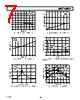
8 / 12 page  AD5551/AD5552 –8– REV. 0 100 90 0% 10 CLOCK (5V/DIV) VOUT (50mV/DIV) 2 s/DIV VREF = 2.5V VDD = 5V TA = 25 C TPC 13. Digital Feedthrough 100 90 0% 10 2µs/DIV VREF = 2.5V VDD = 5V TA = 25 C CS (5V/DIV) VOUT (0.1V/DIV) TPC 14. Digital-to-Analog Glitch Impulse GENERAL DESCRIPTION The AD5551/AD5552 are single, 14-bit, serial input, voltage output DACs. They operate from a single supply ranging from 2.7 V to 5 V and consume typically 300 A with a supply of 5 V. Data is written to these devices in a 14-bit word format, via a 3- or 4-wire serial interface. To ensure a known power-up state, these parts were designed with a power-on reset function. In uni- polar mode, the output is reset to 0 V, while in bipolar mode, the AD5552 output is set to –VREF. Kelvin sense connections for the reference and analog ground are included on the AD5552. Digital-to-Analog Section The DAC architecture consists of two matched DAC sections. A simplified circuit diagram is shown in Figure 2. The DAC architecture of the AD5551/AD5552 is segmented. The four MSBs of the 14-bit data word are decoded to drive 15 switches, E1 to E15. Each of these switches connects one of 15 matched resistors to either AGND or VREF. The remaining 10 bits of the data word drive switches S0 to S9 of a 10-bit voltage mode R-2R ladder network. R VOUT 2R 2R 2R R 2R 2R 2R 2R S0 S1 S9 E1 E2 E15 VREF 10-BIT R-2R LADDER FOUR MSBs DECODED INTO 15 EQUAL SEGMENTS Figure 2. DAC Architecture 100 90 0% 10 VREF = 2.5V VDD = 5V TA = 25 C 10pF 50pF 200pF 100pF 2µs/DIV CS (5V/DIV) VOUT (0.5V/DIV) TPC 15. Large Signal Settling Time VOUT (1V/DIV) VOUT (50mV/DIV) GAIN = –216 100 90 0% 10 VREF = 2.5V VDD = 5V TA = 25 C 0.5 s/DIV TPC 16. Small Signal Settling Time With this type of DAC configuration, the output impedance is independent of code, while the input impedance seen by the ref- erence is heavily code dependent. The output voltage is dependent on the reference voltage as shown in the following equation. V VD OUT REF N = × 2 where D is the decimal data word loaded to the DAC register and N is the resolution of the DAC. For a reference of 2.5 V, the equation simplifies to the following. V D OUT = × 25 16 384 . , giving a VOUT of 1.25 V with midscale loaded, and 2.5 V with full-scale loaded to the DAC. The LSB size is VREF/16,384. Serial Interface The AD5551 and AD5552 are controlled by a versatile 3-wire serial interface, which operates at clock rates up to 25 MHz and is compatible with SPI, QSPI, MICROWIRE, and DSP interface standards. The timing diagram can be seen in Figure 1. Input data is framed by the chip select input, CS. After a high-to-low transition on CS, data is shifted synchronously and latched into the input register on the rising edge of the serial clock, SCLK. Data is loaded MSB first in 14-bit words. After 14 data bits have been loaded into the serial input register, a low-to-high transition on CS transfers the contents of the shift register to the DAC. Data can only be loaded to the part while CS is low. |
|
|
Link URL |
| Lei ha avuto il aiuto da alldatasheet? [ DONATE ] |
Di alldatasheet | Richest di pubblicita | contatti | Privacy Policy | Collegamento alla scheda tecnica | scambio Link | Ricerca produttore All Rights Reserved©Alldatasheet.com |
| Russian : Alldatasheetru.com | Korean : Alldatasheet.co.kr | Spanish : Alldatasheet.es | French : Alldatasheet.fr | Italian : Alldatasheetit.com Portuguese : Alldatasheetpt.com | Polish : Alldatasheet.pl | Vietnamese : Alldatasheet.vn Indian : Alldatasheet.in | Mexican : Alldatasheet.com.mx | British : Alldatasheet.co.uk | New Zealand : Alldatasheet.co.nz |
|
Family Site : ic2ic.com |
icmetro.com |
 Italian ▼
 English
 Chinese
 German
 Japanese
 Russian
 Korean
 Spanish
 French
 Italian
 Portuguese
 Polish
 Vietnamese
 Indian
 Mexican
 British
 New Zealand