|
Motore di ricerca datesheet componenti elettronici |
|
|
Motore di ricerca datesheet componenti elettronici |
|
AD5544ARS Scheda tecnica(PDF) 8 Page - Analog Devices |
|
|
|||||||||||||||||||||||||||||
AD5544ARS Scheda tecnica(HTML) 8 Page - Analog Devices |
|
|
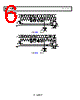
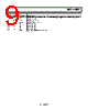
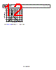
8 / 24 page  AD5544/AD5554 Data Sheet Rev. G | Page 8 of 24 PIN CONFIGURATIONS AND FUNCTION DESCRIPTIONS 28 27 26 25 24 23 22 21 20 19 18 17 16 15 1 2 3 4 5 6 7 8 9 10 11 12 13 14 AD5544/ AD5554 TOP VIEW (Not to Scale) AGNDA AGNDD IOUTA IOUTD VREFA VREFD RFBARFBD MSB DGND VSS VDD AGNDF CLK SDO SDI NC RFBB RFBC VREFB VREFC IOUTB IOUTC AGNDBAGNDC NC = NO CONNECT LDAC CS RS Figure 5. TSSOP Pin Configuration NOTES 1. NC = NO CONNECT. 2. CONNECT EXPOSED PAD TO AGND. 24 DGND 23 VSS 22 AGNDF 21 LDAC 20 SDO 19 NC 18 RFBC 17 VREFC 1 2 3 4 5 6 7 8 AGNDA IOUTA VREFA RFBA MSB RS VDD CS AD5544 TOP VIEW (Not to Scale) Figure 6. LFCSP Pin Configuration Table 4. Pin Function Descriptions TSSOP Pin No. LFCSP Pin No. Mnemonic Description 1 1 AGNDA DAC A Analog Ground. 2 2 IOUTA DAC A Current Output. 3 3 VREFA DAC A Reference Voltage Input Terminal. Establishes DAC A full-scale output voltage. This pin can be tied to the VDD pin. 4 4 RFBA Establish the voltage output for DAC A by connecting to an external amplifier output. 5 5 MSB MSB Bit. Set pin during a reset pulse (RS) or at system power-on if tied to ground or VDD. 6 6 RS Reset Pin, Active Low Input. Input registers and DAC registers are set to all 0s or half-scale code (0x8000 for the AD5544 and 0x2000 for the AD5554), determined by the voltage on the MSB pin. Register data = 0x0000 when MSB = 0. 7 7 VDD Positive Power Supply Input. Specified range of operation: 5 V ± 10%. 8 8 CS Chip Select, Active Low Input. Disables shift register loading when high. Transfers serial register data to the input register when CS/LDAC returns high. Does not affect LDAC operation. 9 9 CLK Clock Input. Positive edge clocks data into the shift register. 10 10 SDI Serial Data Input. Input data loads directly into the shift register. 11 11 RFBB Establish the voltage output for DAC B by connecting to an external amplifier output. 12 12 VREFB DAC B Reference Voltage Input Terminal. Establishes DAC B full-scale output voltage. This pin can be tied to the VDD pin. 13 13 IOUTB DAC B Current Output. 14 14 AGNDB DAC B Analog Ground. 15 15 AGNDC DAC C Analog Ground. 16 16 IOUTC DAC C Current Output. 17 17 VREFC DAC C Reference Voltage Input Terminal. Establishes DAC C full-scale output voltage. This pin can be tied to the VDD pin. 18 18 RFBC Establish the voltage output for DAC C by connecting to an external amplifier output. 19 19 NC No Connect. Leave the pin unconnected. 20 20 SDO Serial Data Output. Input data loads directly into the shift register. Data appears at SDO at 19 clock pulses for the AD5544 and 17 clock pulses for the AD5554 after input at the SDI pin. 21 21 LDAC Load DAC Register Strobe, Level Sensitive Active Low. Transfers all input register data to DAC registers. Asynchronous active low input. See Table 8 and Table 9 for operation. 22 22 AGNDF High Current Analog Force Ground. 23 23 VSS Negative Bias Power Supply Input. Specified range of operation: −5.5 V to +0.3 V. 24 24 DGND Digital Ground Pin. 25 25 RFBD Establish the voltage output for DAC D by connecting to an external amplifier output. |
|
|
Link URL |
| Lei ha avuto il aiuto da alldatasheet? [ DONATE ] |
Di alldatasheet | Richest di pubblicita | contatti | Privacy Policy | Collegamento alla scheda tecnica | scambio Link | Ricerca produttore All Rights Reserved©Alldatasheet.com |
| Russian : Alldatasheetru.com | Korean : Alldatasheet.co.kr | Spanish : Alldatasheet.es | French : Alldatasheet.fr | Italian : Alldatasheetit.com Portuguese : Alldatasheetpt.com | Polish : Alldatasheet.pl | Vietnamese : Alldatasheet.vn Indian : Alldatasheet.in | Mexican : Alldatasheet.com.mx | British : Alldatasheet.co.uk | New Zealand : Alldatasheet.co.nz |
|
Family Site : ic2ic.com |
icmetro.com |
 Italian ▼
 English
 Chinese
 German
 Japanese
 Russian
 Korean
 Spanish
 French
 Italian
 Portuguese
 Polish
 Vietnamese
 Indian
 Mexican
 British
 New Zealand