|
Motore di ricerca datesheet componenti elettronici |
|
|
Motore di ricerca datesheet componenti elettronici |
|
MP8718 Scheda tecnica(PDF) 9 Page - Monolithic Power Systems |
|
|
|||||||||||||||||||||||||||||
MP8718 Scheda tecnica(HTML) 9 Page - Monolithic Power Systems |
|
|
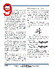
9 / 17 page  MP8718 – SYNCHRONOUS STEP-DOWN CONVERTER WITH INTERNAL MOSFETS MP8718 Rev. 0.9 www.MonolithicPower.com 9 2/9/2010 MPS Proprietary Information. Unauthorized Photocopy and Duplication Prohibited. © 2010 MPS. All Rights Reserved. OPERATION The MP8718 is a high frequency synchronous rectified step-down switch mode converter with built in internal power MOSFETs. It offers a very compact solution to achieve 4A continuous output current over a wide input supply range with excellent load and line regulation. The MP8718 operates in a fixed frequency, peak current control mode to regulate the output voltage. A PWM cycle is initiated by the internal clock. The integrated high-side power MOSFET is turned on and remains on until its current reaches the value set by the COMP voltage. When the power switch is off, it remains off until the next clock cycle starts. If, in 90% of one PWM period, the current in the power MOSFET does not reach the COMP set current value, the power MOSFET will be forced to turn off Internal Regulator Most of the internal circuitries are powered from the 5V internal regulator. This regulator takes the VIN input and operates in the full VIN range. When VIN is greater than 5.0V, the output of the regulator is in full regulation. When VIN is lower than 5.0V, the output decreases, a 0.1uF ceramic capacitor for decoupling purpose is required. Error Amplifier The error amplifier compares the FB pin voltage with the internal 0.805V reference (REF) and outputs a current proportional to the difference between the two. This output current is then used to charge or discharge the internal compensation network to form the COMP voltage, which is used to control the power MOSFET current. The optimized internal compensation network minimizes the external component counts and simplifies the control loop design. Enable/Sync Control EN/Sync is a digital control pin that turns the regulator on and off. Drive EN high to turn on the regulator, drive it low to turn it off. There is an internal 1MEG resistor from EN/Sync to GND thus EN/Sync can be floated to shut down the chip. 1) Enabled by external logic H/L signal The chip starts up once the enable signal goes higher than EN/SYNC input high voltage (2V), and is shut down when the signal is lower than EN/SYNC input low voltage (0.4V). To disable the chip, EN must be pulled low for at least 5µs. The input is compatible with both CMOS and TTL. 2) Enabled by Vin through voltage divider. Connect EN with Vin through a resistive voltage divider for automatic startup as the figure 2 shows. EN VIN REN1 REN2 Figure 2—Enable Divider Circuit Choose the value of the pull-up resistor REN1 and pull-down resistor REN2 to reset the automatic start-up voltage: R R (R V V EN2 EN2 EN1 EN_RISING IN_START Ω Ω + ⋅ = M M 1 || ) 1 || Where VEN_RISING is 1.3V Ω Ω + ⋅ = M M 1 || ) 1 || EN2 EN2 EN1 FALLING - EN IN_STOP R R (R V V Where VEN_FALLING is 0.9V For example, REN1=100kΩ and REN2=20kΩ, the VIN-START is set at 7.9V, VIN-STOP is set at 5.49V. The startup sequence is as below using the EN divider. VCC-Rising is the VCC UVLO rising threshold which is about 4.0V. |
|
|
Link URL |
| Lei ha avuto il aiuto da alldatasheet? [ DONATE ] |
Di alldatasheet | Richest di pubblicita | contatti | Privacy Policy | Collegamento alla scheda tecnica | scambio Link | Ricerca produttore All Rights Reserved©Alldatasheet.com |
| Russian : Alldatasheetru.com | Korean : Alldatasheet.co.kr | Spanish : Alldatasheet.es | French : Alldatasheet.fr | Italian : Alldatasheetit.com Portuguese : Alldatasheetpt.com | Polish : Alldatasheet.pl | Vietnamese : Alldatasheet.vn Indian : Alldatasheet.in | Mexican : Alldatasheet.com.mx | British : Alldatasheet.co.uk | New Zealand : Alldatasheet.co.nz |
|
Family Site : ic2ic.com |
icmetro.com |
 Italian ▼
 English
 Chinese
 German
 Japanese
 Russian
 Korean
 Spanish
 French
 Italian
 Portuguese
 Polish
 Vietnamese
 Indian
 Mexican
 British
 New Zealand