|
Motore di ricerca datesheet componenti elettronici |
|
|
Motore di ricerca datesheet componenti elettronici |
|
ICS5342 Scheda tecnica(PDF) 2 Page - Integrated Circuit Systems |
|
|
|||||||||||||||||||||||||||||
ICS5342 Scheda tecnica(HTML) 2 Page - Integrated Circuit Systems |
|
|
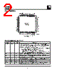
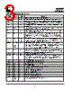
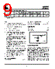
2 / 36 page  ICS5342 GENDAC 2 Pin Configuration Pin Configuration Pin Description (68-pin PLCC) Symbol Pin # Type Description D7 - D0 21-14 I/O Systems data bus bidirectional data I/O lines – used by host microprocessor for internal register read and write operations (using active low RD and WR respec- tively) for six internal registers: Pixel Address, Color Value, Pixel Mask, PLL Address, PLL Parameter, and Command During the write cycle, the rising edge of WR latches the data into the selected register (set by the status of the three RS pins). The rising edge of RD determines the end of the read cycle. The RD set logical high indicates that data I/O lines no longer contain infor- mation from the selected register and will be tri-stated. RD 5 Input RAM/PLL read enable bus control signal – in active low state, any information present on the internal data bus is available on the Data I/O lines, D0-D7 WR 22 Input Active low RAM/PLL write enable bus control signal – controls write timing on microprocessor interface inputs, D0-D7 RS2-RS0 63,24,23 Input Register address select 0 inputs – control selection of one of six internal registers – inputs are sampled on falling edge of active enable signal (RD or WR) XIN 48 Input Crystal input – connect to 14.318 MHz crystal XOUT 49 Output Crystal output – connect to 14.318 MHz crystal MSW 25 Input Mode switch – digital control for selecting primary and secondary pixel color modes – low selects primary mode – connect to ground if not used CGND PCLK P7 P6 P5 P4 P3 P2 P1 P0 XVDD XGND XOUT XIN VREF N/C DGND 5342_02 60 59 58 57 56 55 54 53 52 51 50 49 48 47 46 45 44 GENDAC II ICS5342 D0 D1 D2 D3 D4 D5 CGND CLK1 P14 P15 WR* RS0 RS1 MSW CGND 10 11 12 13 14 15 16 17 18 19 20 21 22 23 24 25 26 D7 D6 ICS5342 (68-pin PLCC) |
|
Link URL |
| Lei ha avuto il aiuto da alldatasheet? [ DONATE ] |
Di alldatasheet | Richest di pubblicita | contatti | Privacy Policy | Collegamento alla scheda tecnica | scambio Link | Ricerca produttore All Rights Reserved©Alldatasheet.com |
| Russian : Alldatasheetru.com | Korean : Alldatasheet.co.kr | Spanish : Alldatasheet.es | French : Alldatasheet.fr | Italian : Alldatasheetit.com Portuguese : Alldatasheetpt.com | Polish : Alldatasheet.pl | Vietnamese : Alldatasheet.vn Indian : Alldatasheet.in | Mexican : Alldatasheet.com.mx | British : Alldatasheet.co.uk | New Zealand : Alldatasheet.co.nz |
|
Family Site : ic2ic.com |
icmetro.com |
 Italian ▼
 English
 Chinese
 German
 Japanese
 Russian
 Korean
 Spanish
 French
 Italian
 Portuguese
 Polish
 Vietnamese
 Indian
 Mexican
 British
 New Zealand