|
Motore di ricerca datesheet componenti elettronici |
|
|
Motore di ricerca datesheet componenti elettronici |
|
LT1724 Scheda tecnica(PDF) 7 Page - Linear Technology |
|
|
|||||||||||||||||||||||||||||
LT1724 Scheda tecnica(HTML) 7 Page - Linear Technology |
|
|
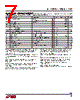
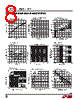
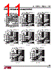
7 / 18 page  LT1722/LT1723/LT1724 7 172234fb ELECTRICAL CHARACTERISTICS The ● denotes the specifications which apply over the temperature range of –40°C ≤ TA ≤ 85°C. VS = 5V, VCM = 2.5V, RL to 2.5V, unless otherwise noted. (Note 5) Note 1: Stresses beyond those listed under Absolute Maximum Ratings may cause permanent damage to the device. Exposure to any Absolute Maximum Rating condition for extended periods may affect device reliability and lifetime. Note 2: The inputs are protected by back-to-back diodes. If the differential input voltage exceeds 0.7V, the input current should be limited to less than 10mA. Note 3: A heat sink may be required to keep the junction temperature below the absolute maximum rating when the output is shorted indefinitely. Note 4: The LT1722C/LT1722I, LT1723C/LT1723I, LT1724C/LT1724I are guaranteed functional over the operating temperature range of –40°C to 85°C. Note 5: The LT1722C/LT1723C/LT1724C are guaranteed to meet specified performance from 0°C to 70°C. The LT1722C/LT1723C/LT1724C are SYMBOL PARAMETER CONDITIONS MIN TYP MAX UNITS VOS Input Offset Voltage (Note 6) LT1722 SOT-23 and LT1723 MS8 l l 1000 1200 µV µV Input VOS Drift (Note 9) l 310 μV/°C IOS Input Offset Current l 400 nA IB Input Bias Current l 400 nA Input Voltage Range + Input Voltage Range – l l 3.5 1.5 V V CMRR Common Mode Rejection Ratio VCM = 1.5V to 3.5V l 75 dB AVOL Large-Signal Voltage Gain VOUT = 1.5V to 3.5V, RL = 500Ω l 2 V/mV VOUT Output Swing+ Output Swing– RL = 500Ω, VIN = ±10mV RL = 500Ω, VIN = ±10mV l l 3.5 1.5 V V IOUT Output Current VOUT = 3.5V or 1.5V, 30mV Overdrive l 8mA ISC Short-Circuit Current VOUT = 2.5V, VIN = ±1V l 10 mA SR Slew Rate AV = –1, (Note 7) l 20 V/μs GBW Gain Bandwidth (Note 10) f = 200kHz l 90 MHz Channel Separation VOUT = 1.5V to 3.5V, RL = 500Ω l 80 dB IS Supply Current l 6.45 mA designed, characterized and expected to meet specified performance from –40°C to 85°C but are not tested or QA sampled at these temperatures. The LT1722I/LT1723I/LT1724I are guaranteed to meet specified performance from –40°C to 85°C. Note 6: Input offset voltage is pulse tested and is exclusive of warm-up drift. Note 7: Slew rate is measured between ±2V on the output with ±3V input for ±5V supplies and ±1V on the output with ±1.5V input for single 5V supply. (For 5V supply, the voltage levels are 2.5V referred.) Note 8: Full power bandwidth is calculated from the slew rate: FPBW = SR/2πVP Note 9 : This parameter is not 100% tested. Note 10 : This parameter is guaranteed through correlation with slew rate. |
|
|
Link URL |
| Lei ha avuto il aiuto da alldatasheet? [ DONATE ] |
Di alldatasheet | Richest di pubblicita | contatti | Privacy Policy | Collegamento alla scheda tecnica | scambio Link | Ricerca produttore All Rights Reserved©Alldatasheet.com |
| Russian : Alldatasheetru.com | Korean : Alldatasheet.co.kr | Spanish : Alldatasheet.es | French : Alldatasheet.fr | Italian : Alldatasheetit.com Portuguese : Alldatasheetpt.com | Polish : Alldatasheet.pl | Vietnamese : Alldatasheet.vn Indian : Alldatasheet.in | Mexican : Alldatasheet.com.mx | British : Alldatasheet.co.uk | New Zealand : Alldatasheet.co.nz |
|
Family Site : ic2ic.com |
icmetro.com |
 Italian ▼
 English
 Chinese
 German
 Japanese
 Russian
 Korean
 Spanish
 French
 Italian
 Portuguese
 Polish
 Vietnamese
 Indian
 Mexican
 British
 New Zealand