|
Motore di ricerca datesheet componenti elettronici |
|
|
Motore di ricerca datesheet componenti elettronici |
|
LT1124 Scheda tecnica(PDF) 9 Page - Linear Technology |
|
|
|||||||||||||||||||||||||||||
LT1124 Scheda tecnica(HTML) 9 Page - Linear Technology |
|
|
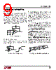
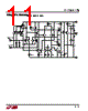
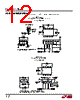
9 / 16 page  9 LT1124/LT1125 High Speed Operation When the feedback around the op amp is resistive (RF), a pole will be created with RF, the source resistance and capacitance (RS, CS), and the amplifier input capacitance (CIN ≈ 2pF). In low closed loop gain configurations and with RS and RF in the kilohm range, this pole can create excess phase shift and even oscillation. A small capacitor (CF) in parallel with RF eliminates this problem (see Figure 2). With RS (CS + CIN) = RFCF, the effect of the feedback pole is completely removed. During the fast feedthrough-like portion of the output, the input protection diodes effectively short the output to the input and a current, limited only by the output short circuit protection, will be drawn by the signal generator. With RF ≥500Ω, the output is capable of handling the current requirements (IL ≤ 20mA at 10V) and the amplifier stays in its active mode and a smooth transition will occur. Noise Testing Each individual amplifier is tested to 4.2nV/ √Hz voltage noise; i.e., for the LT1124 two tests, for the LT1125 four tests are performed. Noise testing for competing multiple op amps, if done at all, may be sample tested or tested using the circuit shown in Figure 4. en OUT = √(enA)2 + (enB)2 + (enC)2 + (enD)2 If the LT1125 were tested this way, the noise limit would be √ 4 • (4.2nV/√Hz)2 = 8.4nV/√Hz. But is this an effective screen? What if three of the four amplifiers are at a typical 2.7nV/ √Hz, and the fourth one was contaminated and has 6.9nV/ √Hz noise? RMS Sum = √(2.7)2 + (2.7)2 + (2.7)2 + (6.9)2 = 8.33nV/√Hz This passes an 8.4nV/ √Hz spec, yet one of the amplifiers is 64% over the LT1125 spec limit. Clearly, for proper noise measurement, the op amps have to be tested individually. S APPLICATI I FOR ATIO + – 1124/25 F03 OUTPUT 4.5V/ µs RF Figure 3. Unity-Gain Buffer Applications 1124/25 F04 + – A + – B + – C + – D OUT Figure 4. Competing Quad Op Amp Noise Test Method – + OUTPUT 1124/25 F02 RS CS RF CF CIN Figure 2. High Speed Operation Unity Gain Buffer Applications When RF ≤ 100Ω and the input is driven with a fast, large signal pulse (>1V), the output waveform will look as shown in Figure 3. |
|
|
Link URL |
| Lei ha avuto il aiuto da alldatasheet? [ DONATE ] |
Di alldatasheet | Richest di pubblicita | contatti | Privacy Policy | Collegamento alla scheda tecnica | scambio Link | Ricerca produttore All Rights Reserved©Alldatasheet.com |
| Russian : Alldatasheetru.com | Korean : Alldatasheet.co.kr | Spanish : Alldatasheet.es | French : Alldatasheet.fr | Italian : Alldatasheetit.com Portuguese : Alldatasheetpt.com | Polish : Alldatasheet.pl | Vietnamese : Alldatasheet.vn Indian : Alldatasheet.in | Mexican : Alldatasheet.com.mx | British : Alldatasheet.co.uk | New Zealand : Alldatasheet.co.nz |
|
Family Site : ic2ic.com |
icmetro.com |
 Italian ▼
 English
 Chinese
 German
 Japanese
 Russian
 Korean
 Spanish
 French
 Italian
 Portuguese
 Polish
 Vietnamese
 Indian
 Mexican
 British
 New Zealand