|
Motore di ricerca datesheet componenti elettronici |
|
|
Motore di ricerca datesheet componenti elettronici |
|
TLV2211CDBVT Scheda tecnica(PDF) 26 Page - Texas Instruments |
|
|
|
|||||||||||||||||||||||||||||
TLV2211CDBVT Scheda tecnica(HTML) 26 Page - Texas Instruments |
|
|
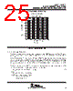
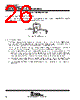
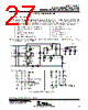
26 / 31 page  TLV2211, TLV2211Y Advanced LinCMOS RAILTORAIL MICROPOWER SINGLE OPERATIONAL AMPLIFIERS SLOS156E − MAY 1996 − REVISED SEPTEMBER 2006 26 POST OFFICE BOX 655303 • DALLAS, TEXAS 75265 APPLICATION INFORMATION driving large capacitive loads (continued) The unity-gain bandwidth (UGBW) frequency decreases as the capacitive load increases (see Figure 54). To use equation 1, UGBW must be approximated from Figure 54. 10 k Ω 10 k Ω VDD −/ GND VDD + Rnull CL VI + − Figure 54. Series-Resistance Circuit driving heavy dc loads The TLV2211 is designed to provide better sinking and sourcing output currents than earlier CMOS rail-to-rail output devices. This device is specified to sink 500 µA and source 250 µA at VDD = 3 V and VDD = 5 V at a maximum quiescent IDD of 25 µA. This provides a greater than 90% power efficiency. When driving heavy dc loads, such as 10 k Ω, the positive edge can experience some distortion under slewing conditions. This condition can be seen in Figure 39. This condition is affected by three factors: D Where the load is referenced. When the load is referenced to either rail, this condition does not occur. The distortion occurs only when the output signal swings through the point where the load is referenced. Figure 40 illustrates two 10-k Ω load conditions. The first load condition shows the distortion seen for a 10-k Ω load tied to 2.5 V. The third load condition shows no distortion for a 10-kΩ load tied to 0 V. D Load resistance. As the load resistance increases, the distortion seen on the output decreases. Figure 40 illustrates the difference seen on the output for a 10-k Ω load and a 100-kΩ load with both tied to 2.5 V. D Input signal edge rate. Faster input edge rates for a step input result in more distortion than with slower input edge rates. |
|
Link URL |
| Lei ha avuto il aiuto da alldatasheet? [ DONATE ] |
Di alldatasheet | Richest di pubblicita | contatti | Privacy Policy | Collegamento alla scheda tecnica | scambio Link | Ricerca produttore All Rights Reserved©Alldatasheet.com |
| Russian : Alldatasheetru.com | Korean : Alldatasheet.co.kr | Spanish : Alldatasheet.es | French : Alldatasheet.fr | Italian : Alldatasheetit.com Portuguese : Alldatasheetpt.com | Polish : Alldatasheet.pl | Vietnamese : Alldatasheet.vn Indian : Alldatasheet.in | Mexican : Alldatasheet.com.mx | British : Alldatasheet.co.uk | New Zealand : Alldatasheet.co.nz |
|
Family Site : ic2ic.com |
icmetro.com |
 Italian ▼
 English
 Chinese
 German
 Japanese
 Russian
 Korean
 Spanish
 French
 Italian
 Portuguese
 Polish
 Vietnamese
 Indian
 Mexican
 British
 New Zealand