|
Motore di ricerca datesheet componenti elettronici |
|
|
Motore di ricerca datesheet componenti elettronici |
|
ML610Q461 Scheda tecnica(PDF) 13 Page - LAPIS Semiconductor Co., Ltd. |
|
|
|||||||||||||||||||||||||||||
ML610Q461 Scheda tecnica(HTML) 13 Page - LAPIS Semiconductor Co., Ltd. |
|
|
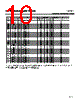
13 / 29 page  FEDL610Q461-03 ML610Q461/ML610Q462/ML610Q463 13/29 Pin name I/O Description Primary/ Secondary/ Tertiary Logic RC oscillation type A/D converter IN0 I Channel 0 oscillation input pin. This pin is used as the secondary function of the P30 pin. Secondary — CS0 O Channel 0 reference capacitor connection pin. This pin is used as the secondary function of the P31 pin. Secondary — RCT0 O Resistor/capacitor sensor connection pin of Channel 0 for measurement. This pin is used as the secondary function of the P33 pin. Secondary — RS0 O This pin is used as the secondary function of the P32 pin which is the reference resistor connection pin of Channel 0. Secondary — RT0 O Resistor sensor connection pin of Channel 0 for measurement. This pin is used as the secondary function of the P34 pin. Secondary — RCM O RC oscillation monitor pin. This pin is used as the secondary function of the P35 pin. Secondary — IN1 I Oscillation input pin of Channel 1. This pin is used as the secondary function of the P44 pin. Secondary — CS1 O Reference capacitor connection pin of Channel 1. This pin is used as the secondary function of the P45 pin. Secondary — RS1 O Reference resistor connection pin of Channel 1. This pin is used as the secondary function of the P46 pin. Secondary — RT1 O Resistor sensor connection pin for measurement of Channel 1. This pin is used as the secondary function of the P47 pin. Secondary — LCD drive signal COM0-3 O Common output pins. — — SEG8-23 O Segment output pins. — — SEG24-27 O Segment output pins. Incorporated into ML610Q462/ML610Q463, not into ML610Q461. — — SEG28-31 O Segment output pins. Incorporated into ML610Q463, not into ML610Q461/ML610Q462. — — LCD driver power supply VL1 — Power supply pins for LCD bias (internally generated or positive power supply pin connected ). Depending on LCD Bias setting and VDD voltage level, VDD or VDDL or capacitor is connected. For details of the connection method, see user’s manual. — — VL2 — — — VL3 — — — C1 — Power supply pins for LCD bias (internally generated). Capacitors C12 is connected between C1 and C2. — — C2 — — — For testing TEST0 I/O Input/output pin for testing. A pull-down resistor is internally connected. — — TEST1_N I Input pin for testing. A pull-up resistor is internally connected. — — Power supply VSS — Negative power supply pin. — — VDD — Positive power supply pin for I/O, internal regulator, battery low detector, and power-on reset. — — VDDL — Positive power supply pin (internally generated) for internal logic. Capacitor CL (see measuring circuit 1) is connected between this pin and VSS. — — VPP — Power supply pin for programming Flash ROM. A pull-down resistor is internally connected. — — |
|
Link URL |
| Lei ha avuto il aiuto da alldatasheet? [ DONATE ] |
Di alldatasheet | Richest di pubblicita | contatti | Privacy Policy | Collegamento alla scheda tecnica | scambio Link | Ricerca produttore All Rights Reserved©Alldatasheet.com |
| Russian : Alldatasheetru.com | Korean : Alldatasheet.co.kr | Spanish : Alldatasheet.es | French : Alldatasheet.fr | Italian : Alldatasheetit.com Portuguese : Alldatasheetpt.com | Polish : Alldatasheet.pl | Vietnamese : Alldatasheet.vn Indian : Alldatasheet.in | Mexican : Alldatasheet.com.mx | British : Alldatasheet.co.uk | New Zealand : Alldatasheet.co.nz |
|
Family Site : ic2ic.com |
icmetro.com |
 Italian ▼
 English
 Chinese
 German
 Japanese
 Russian
 Korean
 Spanish
 French
 Italian
 Portuguese
 Polish
 Vietnamese
 Indian
 Mexican
 British
 New Zealand