|
Motore di ricerca datesheet componenti elettronici |
|
|
Motore di ricerca datesheet componenti elettronici |
|
IS24C64 Scheda tecnica(PDF) 2 Page - Integrated Silicon Solution, Inc |
|
|
|||||||||||||||||||||||||||||
IS24C64 Scheda tecnica(HTML) 2 Page - Integrated Silicon Solution, Inc |
|
|
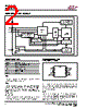
2 / 11 page  2 Integrated Silicon Solution, Inc. — 1-800-379-4774 PRELIMINARY INFORMATION Rev. 00B 04/04/01 IS24C32-2/3 IS24C64-2/3 ISSI® > CONTROL LOGIC SLAVE ADDRESS REGISTER & COMPARATOR WORD ADDRESS COUNTER HIGH VOLTAGE GENERATOR, TIMING & CONTROL EEPROM ARRAY Y DECODER DATA REGISTER Clock DI/O ACK 8 5 6 7 4 GND WP SCL SDA Vcc nMOS PIN DESCRIPTIONS A0-A2 Address Inputs SDA Serial Address/Data I/O SCL Serial Clock Input WP Write Protect Input Vcc Power Supply GND Ground SCL This input clock pin is used to synchronize the data transfer to and from the device. SDA The SDA is a Bi-directional pin used to transfer addresses and data into and out of the device. The SDA pin is an open drain output and can be wire-Ored with other open drain or open collector outputs. The SDA bus requires a pullup resistor to Vcc. A0, A1, A2 The A0, A1 and A2 are the device address inputs that are hardwired or left not connected for hardware compatibility PIN CONFIGURATION 8-Pin DIP and SOIC 1 2 3 4 8 7 6 5 A0 A1 A2 GND VCC WP SCL SDA FUNCTIONAL BLOCK DIAGRAM with the 24C16. When pins are hardwired, as many as eight 32K/64K devices may be addressed on a single bus system. When the pins are not hardwired, the default A0, A1,and A2 are zero.. WP WP is the Write Protect pin. If the WP pin is tied to Vcc the entire array becomes Write Protected (Read only). When WP is tied to GND or left floating normal read/write operations are allowed to the device. |
|
|
Link URL |
| Lei ha avuto il aiuto da alldatasheet? [ DONATE ] |
Di alldatasheet | Richest di pubblicita | contatti | Privacy Policy | Collegamento alla scheda tecnica | scambio Link | Ricerca produttore All Rights Reserved©Alldatasheet.com |
| Russian : Alldatasheetru.com | Korean : Alldatasheet.co.kr | Spanish : Alldatasheet.es | French : Alldatasheet.fr | Italian : Alldatasheetit.com Portuguese : Alldatasheetpt.com | Polish : Alldatasheet.pl | Vietnamese : Alldatasheet.vn Indian : Alldatasheet.in | Mexican : Alldatasheet.com.mx | British : Alldatasheet.co.uk | New Zealand : Alldatasheet.co.nz |
|
Family Site : ic2ic.com |
icmetro.com |
 Italian ▼
 English
 Chinese
 German
 Japanese
 Russian
 Korean
 Spanish
 French
 Italian
 Portuguese
 Polish
 Vietnamese
 Indian
 Mexican
 British
 New Zealand