 |
Motore di ricerca datesheet componenti elettronici |
|
|
Motore di ricerca datesheet componenti elettronici |
|
The question interval is too short.
Please try again in a few seconds.

Hello, Please ask a question about GD25LH40C Datasheet
# Example questions:
➢ Comparing tables 1 & 2, what is the maximum size (in kb) of a single memory block that can be protected using the bp settings in table 1a?
➢ If you set bp4=0, bp3=0, bp2=1, bp1=0, and bp0=1, which memory blocks are *not* protected?
➢ If bp4=1, bp3=0, bp2=0, bp1=0, and bp0=0, what portion of the memory is protected?
| Part No. | GD25LH40C |
| Manufacturer | GIGADEVICE |
| Size | 1Mb |
| Pages | 69 pages |
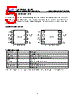
| Description | 1.8V Uniform Sector Dual and Quad Serial Flash |








Okay, let's break down the information presented in these extracts from the GD25LH series Flash memory datasheet. This is a complex topic, but I'm going to summarize the key points.
1. General Information - GD25LH Series (Likely GD25LH40C, GD25LH20C, GD25LH10C)
️· What they are: These are Flash memory devices. Flash memory is a type of non-volatile memory – it retains data even when power is removed.
️· Likely Denominations: The text refers to GD25LH40C, GD25LH20C, and GD25LH10C. The '40C' likely refers to a 4Mb (4096kb) density, '20C' to 2Mb (2048kb), and '10C' to 1Mb(1024kb).
️· Uniform Sector: The term "uniform sector" implies a standard size block of memory being written and erased, simplifying the memory management.
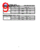
2. Protected Area Size Tables (CMP=0 and CMP=1)
️· What they do: These tables define how memory blocks can be protected from writing. This is a security feature to prevent accidental or malicious modification of critical data.
️· `CMP` Register: The tables are presented for two different CMP register values, 0 and 1. This register likely controls some aspect of the memory protection mechanism.
️· `BP4`, `BP3`, `BP2`, `BP1`, `BP0`: These are bits within a register (likely a status or configuration register). The combination of these bits determines which memory blocks are protected.
️· `Blocks`: Indicates the number of blocks protected.
️· `Addresses`: Lists the starting memory address of the protected area. This is expressed in hexadecimal format (e.g., `000000H` is memory address 0).
️· `Density`: Refers to the total memory capacity (e.g., 64KB, 128KB, 256KB).
️· `Portion`: Describes the fraction of memory that is protected based on the register settings (e.g., Upper 1/2, Lower 1/8).
️· The Tables are Complex: Interpreting these tables requires understanding the register map and how the bits interact. There are several combinations, each defining different protected areas.
Specific Table Differences:
️· GD25LH40C (CMP=0 and CMP=1): Offers the most granular protection options, with various block sizes and addresses. The CMP=1 table has fewer protection options.
️· GD25LH20C (CMP=0 and CMP=1): Offers fewer protection options than the 40C.
️· GD25LH10C: No tables are provided for this, so its protected area functionality might be simpler or require a different mechanism.
Key Takeaways & What You'll Need to Understand This Fully:
️· Register Map: You're missing the crucial register map that explains what each bit in the status register means.
️· Memory Organization: You need to know how memory is organized into blocks and sectors to understand the addresses and portions.
️· CMP Register: The specific function of the CMP register needs to be known. It's the key to understanding the impact of CMP=0 vs CMP=1.
To use these tables effectively, you would need to:
1. Identify the target device: Determine which specific GD25LH model you are working with (e.g., GD25LH40C, GD25LH20C, GD25LH10C).
2. Consult the full datasheet: Refer to the complete datasheet for the device to understand the register map, memory organization, and how to configure the protected areas.
3. Experiment: Test different register configurations to verify the protected areas and ensure they work as expected.
Let me know if you have other extracts or specific questions about these tables.
1. General Information - GD25LH Series (Likely GD25LH40C, GD25LH20C, GD25LH10C)
️· What they are: These are Flash memory devices. Flash memory is a type of non-volatile memory – it retains data even when power is removed.
️· Likely Denominations: The text refers to GD25LH40C, GD25LH20C, and GD25LH10C. The '40C' likely refers to a 4Mb (4096kb) density, '20C' to 2Mb (2048kb), and '10C' to 1Mb(1024kb).
️· Uniform Sector: The term "uniform sector" implies a standard size block of memory being written and erased, simplifying the memory management.
2. Protected Area Size Tables (CMP=0 and CMP=1)
️· What they do: These tables define how memory blocks can be protected from writing. This is a security feature to prevent accidental or malicious modification of critical data.
️· `CMP` Register: The tables are presented for two different CMP register values, 0 and 1. This register likely controls some aspect of the memory protection mechanism.
️· `BP4`, `BP3`, `BP2`, `BP1`, `BP0`: These are bits within a register (likely a status or configuration register). The combination of these bits determines which memory blocks are protected.
️· `Blocks`: Indicates the number of blocks protected.
️· `Addresses`: Lists the starting memory address of the protected area. This is expressed in hexadecimal format (e.g., `000000H` is memory address 0).
️· `Density`: Refers to the total memory capacity (e.g., 64KB, 128KB, 256KB).
️· `Portion`: Describes the fraction of memory that is protected based on the register settings (e.g., Upper 1/2, Lower 1/8).
️· The Tables are Complex: Interpreting these tables requires understanding the register map and how the bits interact. There are several combinations, each defining different protected areas.
Specific Table Differences:
️· GD25LH40C (CMP=0 and CMP=1): Offers the most granular protection options, with various block sizes and addresses. The CMP=1 table has fewer protection options.
️· GD25LH20C (CMP=0 and CMP=1): Offers fewer protection options than the 40C.
️· GD25LH10C: No tables are provided for this, so its protected area functionality might be simpler or require a different mechanism.
Key Takeaways & What You'll Need to Understand This Fully:
️· Register Map: You're missing the crucial register map that explains what each bit in the status register means.
️· Memory Organization: You need to know how memory is organized into blocks and sectors to understand the addresses and portions.
️· CMP Register: The specific function of the CMP register needs to be known. It's the key to understanding the impact of CMP=0 vs CMP=1.
To use these tables effectively, you would need to:
1. Identify the target device: Determine which specific GD25LH model you are working with (e.g., GD25LH40C, GD25LH20C, GD25LH10C).
2. Consult the full datasheet: Refer to the complete datasheet for the device to understand the register map, memory organization, and how to configure the protected areas.
3. Experiment: Test different register configurations to verify the protected areas and ensure they work as expected.
| Part No. | GD25LH40C |
| Manufacturer | GIGADEVICE |
| Size | 1Mb |
| Pages | 69 pages |
| Description | 1.8V Uniform Sector Dual and Quad Serial Flash |
| Lei ha avuto il aiuto da alldatasheet? [ DONATE ] |
Di alldatasheet | Richest di pubblicita | contatti | Privacy Policy | Collegamento alla scheda tecnica | scambio Link | Ricerca produttore All Rights Reserved©Alldatasheet.com |
| Russian : Alldatasheetru.com | Korean : Alldatasheet.co.kr | Spanish : Alldatasheet.es | French : Alldatasheet.fr | Italian : Alldatasheetit.com Portuguese : Alldatasheetpt.com | Polish : Alldatasheet.pl | Vietnamese : Alldatasheet.vn Indian : Alldatasheet.in | Mexican : Alldatasheet.com.mx | British : Alldatasheet.co.uk | New Zealand : Alldatasheet.co.nz |
|
Family Site : ic2ic.com |
icmetro.com |
 Italian ▼
  English
 Chinese
 German
 Japanese
 Russian
 Korean
 Spanish
 French
 Portuguese
 Polish
 Vietnamese
 Indian
 Mexican
 British
 New Zealand