 |
Motore di ricerca datesheet componenti elettronici |
|
|
Motore di ricerca datesheet componenti elettronici |
|
The question interval is too short.
Please try again in a few seconds.

Hello, Please ask a question about TC7107 Datasheet
# Example questions:
➢ Explain the fundamental principle of the dual-slope conversion technique, specifically outlining the two phases involved and how they relate to determining the input signal.
➢ What two capacitor values are recommended for use with the auto-zero circuit, and what input signal ranges do they correspond to?
➢ What is the primary benefit of using an integrating adc like the tc7106a/tc7107a in a noisy environment, and how does it achieve this?
| Part No. | TC7107 |
| Manufacturer | MICROCHIP |
| Size | 623 Kbytes |
| Pages | 26 pages |
| Description | 3-1/2 Digit Analog-to-Digital Converters |


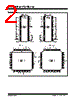

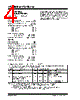
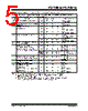


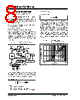




1. Device Overview
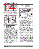
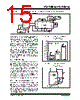
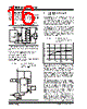
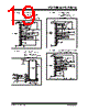
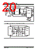
️· What they are: The TC7106A and TC7107A are dual-slope, integrating analog-to-digital converters (ADCs). They's designed for LCD display driving.
️· Dual-Slope Principle: They use a unique method. They integrate the input signal for a set time and then integrate a reference voltage until the integrator returns to zero. The time taken for the reference integration directly relates to the input signal's value.
️· Key Feature: Noise Immunity: The dual-slope technique is remarkably resistant to noise. Noise spikes are effectively averaged out during the integration phases. They're particularly good in environments with electrical interference.
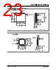
️· Package: Designed for 40-pin PDIP packages.
2. Pin Functions (Important for Wiring!)
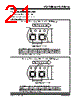
| Pin Number (Normal) | Pin Number (Reversed) | Symbol | Description |
|---|---|---|---|
| 1 | 40 | V+ | Positive supply voltage |
| 9 | 32 | VIN- | Analog LOW input |
| 10 | 31 | VIN+ | Analog HIGH input |
| 32 | 9 | ANALOG COMMON | Sets the Analog Common mode voltage (important for battery operation). |
| 36 | 5 | VREF+ | Reference voltage input for full-scale measurement. |
| 27 | 15 | VINT | Integrator output. Connection for integration capacitor. |
| 39 | 2 | OSC2 | Part of the oscillator circuit. |
| 29 | 12 | CAZ | Auto-zero capacitor connection – crucial for noise performance. |
| 40 | 1 | OSC1 | Oscillator circuit. |
| 21 | 20 | BP/GND | LCD Backplane drive output (TC7106A). Digital Ground (TC7107A). |
| 7 | 34 | CREF- | Reference Capacitor Negative connection |
| 34 | 7 | CREF+ | Reference Capacitor Positive connection |
1. Device Overview
️· What they are: The TC7106A and TC7107A are dual-slope, integrating analog-to-digital converters (ADCs). They's designed for LCD display driving.
️· Dual-Slope Principle: They use a unique method. They integrate the input signal for a set time and then integrate a reference voltage until the integrator returns to zero. The time taken for the reference integration directly relates to the input signal's value.
️· Key Feature: Noise Immunity: The dual-slope technique is remarkably resistant to noise. Noise spikes are effectively averaged out during the integration phases. They're particularly good in environments with electrical interference.
️· Package: Designed for 40-pin PDIP packages.
2. Pin Functions (Important for Wiring!)
| Pin Number (Normal) | Pin Number (Reversed) | Symbol | Description |
|---|---|---|---|
| 1 | 40 | V+ | Positive supply voltage |
| 9 | 32 | VIN- | Analog LOW input |
| 10 | 31 | VIN+ | Analog HIGH input |
| 32 | 9 | ANALOG COMMON | Sets the Analog Common mode voltage (important for battery operation). |
| 36 | 5 | VREF+ | Reference voltage input for full-scale measurement. |
| 27 | 15 | VINT | Integrator output. Connection for integration capacitor. |
| 39 | 2 | OSC2 | Part of the oscillator circuit. |
| 29 | 12 | CAZ | Auto-zero capacitor connection – crucial for noise performance. |
| 40 | 1 | OSC1 | Oscillator circuit. |
| 21 | 20 | BP/GND | LCD Backplane drive output (TC7106A). Digital Ground (TC7107A). |
| 7 | 34 | CREF- | Reference Capacitor Negative connection |
| 34 | 7 | CREF+ | Reference Capacitor Positive connection |
| Part No. | TC7107 |
| Manufacturer | MICROCHIP |
| Size | 623 Kbytes |
| Pages | 26 pages |
| Description | 3-1/2 Digit Analog-to-Digital Converters |
| Lei ha avuto il aiuto da alldatasheet? [ DONATE ] |
Di alldatasheet | Richest di pubblicita | contatti | Privacy Policy | Collegamento alla scheda tecnica | scambio Link | Ricerca produttore All Rights Reserved©Alldatasheet.com |
| Russian : Alldatasheetru.com | Korean : Alldatasheet.co.kr | Spanish : Alldatasheet.es | French : Alldatasheet.fr | Italian : Alldatasheetit.com Portuguese : Alldatasheetpt.com | Polish : Alldatasheet.pl | Vietnamese : Alldatasheet.vn Indian : Alldatasheet.in | Mexican : Alldatasheet.com.mx | British : Alldatasheet.co.uk | New Zealand : Alldatasheet.co.nz |
|
Family Site : ic2ic.com |
icmetro.com |
 Italian ▼
  English
 Chinese
 German
 Japanese
 Russian
 Korean
 Spanish
 French
 Portuguese
 Polish
 Vietnamese
 Indian
 Mexican
 British
 New Zealand