|
Motore di ricerca datesheet componenti elettronici |
|
|
Motore di ricerca datesheet componenti elettronici |
|
ADA4625-2ARDZ-R7 Scheda tecnica(PDF) 23 Page - Analog Devices |
|
|
|||||||||||||||||||||||||||||
ADA4625-2ARDZ-R7 Scheda tecnica(HTML) 23 Page - Analog Devices |
|
|
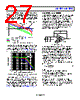
23 / 35 page  Data Sheet ADA4625-1/ADA4625-2 Rev. A | Page 23 of 35 THEORY OF OPERATION Figure 87 shows the simplified circuit diagram for the ADA4625-1/ADA4625-2. The JFET input stage architecture offers the advantages of low input bias current, high bandwidth, high gain, low noise, and no phase reversal when the applied input signal exceeds the common-mode voltage range. The output stage is rail to rail with high drive characteristics and low dropout voltage for both sinking and sourcing currents. INPUT AND GAIN STAGES To achieve high input impedance, low noise, low offset, and low offset drift, the ADA4625-1/AD4625-2A uses large input N channel JFETs (M1 and M2). These JFETs operate with the S source at about 1.2 V above the G gate. In the worst case, the source is only 0.9 V above the gate. By design, the normal operation of the input tail current (ITAIL) extends down to 0.6 V above V−, which gives the ADA4625-1/ADA4625-2 an input common-mode range down to 0.2 V below V− with margin. Resistive loads keep the noise low. The BUFF1 buffer drives the top of the input load resistors (R1 and R2), keeping the voltage drop across M1 and M2 nearly constant, making a virtual cascode. The differences of the input voltages of +IN and –IN steer ITAIL through M1 and M2 to R1 and R2, generating a differential voltage. The first voltage to current gain block (GM1) translates that differential voltage into differential currents (I1 and I2) that drive the current mirror (Q1 and Q2), which generates a differential voltage between the reference node and gain node. JFET inputs of the second voltage to current gain block (GM2) maximizes the gain node impedance, giving the ADA4625-1/ADA4625-2 a high gain. OUTPUT STAGE The GM2 gain block generates two pairs of differential currents. One pair drives the bottom current mirror (Q3 and Q4) and the NPN output transistor (Q7), and the second pair drives the top current mirror (Q5 and Q6) and the output PNP transistor (Q8). The common emitter output transistors (Q7 and Q8) source and sink current rail to rail. GM2 also senses the base voltages of Q7 and Q8 and adjusts the I4 and I6 currents; with no output load, Q7 and Q8 collector currents are 0.6 mA. In addition, GM2 clamps the base voltages of Q7 and Q8 so neither completely turns off. +IN +IN V– V+ INPUT TAIL CURRENT –IN OUT TCVOS TRIM JFET INPUT PAIR 5 V LEVEL SHIFT D G G D S G G D S D S S M4 M3 M1 M2 Q10 I1 I2 I5 I6 I3 I4 BIAS ITC1 ITAIL ITC2 Q9 Q1 CCOMP2 CCOMP1 OUTPUT PNP OUTPUT NPN Q2 –IN GM1 R2 R1 DIFFERENTIAL VOLTAGE INPUT LOAD RESISTORS AND VOS TRIM DIFFERENTIAL CURRENTS GAIN NODE REF NODE V/I GAIN BUFF1 Q3 Q4 Q7 Q8 Q5 Q6 GM2 V/I GAIN AND OUTPUT BIAS Figure 87. Simplified Circuit Diagram |
|
Link URL |
| Lei ha avuto il aiuto da alldatasheet? [ DONATE ] |
Di alldatasheet | Richest di pubblicita | contatti | Privacy Policy | Collegamento alla scheda tecnica | scambio Link | Ricerca produttore All Rights Reserved©Alldatasheet.com |
| Russian : Alldatasheetru.com | Korean : Alldatasheet.co.kr | Spanish : Alldatasheet.es | French : Alldatasheet.fr | Italian : Alldatasheetit.com Portuguese : Alldatasheetpt.com | Polish : Alldatasheet.pl | Vietnamese : Alldatasheet.vn Indian : Alldatasheet.in | Mexican : Alldatasheet.com.mx | British : Alldatasheet.co.uk | New Zealand : Alldatasheet.co.nz |
|
Family Site : ic2ic.com |
icmetro.com |
 Italian ▼
 English
 Chinese
 German
 Japanese
 Russian
 Korean
 Spanish
 French
 Italian
 Portuguese
 Polish
 Vietnamese
 Indian
 Mexican
 British
 New Zealand