|
Motore di ricerca datesheet componenti elettronici |
|
|
Motore di ricerca datesheet componenti elettronici |
|
MCP6476T Scheda tecnica(PDF) 15 Page - Microchip Technology |
|
|
|||||||||||||||||||||||||||||
MCP6476T Scheda tecnica(HTML) 15 Page - Microchip Technology |
|
|
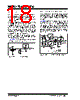
15 / 46 page  2020-2021 Microchip Technology Inc. DS20006419B-page 15 MCP6476/6R/6U/7/9 4.0 APPLICATION INFORMATION The MCP6476/6R/6U/7/9 operational amplifier is unity gain stable and suitable for a wide range of general purpose applications. 4.1 Rail-to-Rail Input 4.1.1 PHASE REVERSAL The MCP6476/6R/6U/7/9 op amp is designed to prevent phase reversal when the input pins exceed the supply voltages. Figure 2-37 shows the input voltage exceeding the supply voltage with no phase reversal. 4.1.2 INPUT VOLTAGE LIMITS In order to prevent damage and/or improper operation of the amplifier, the circuit must limit the voltages at the input pins (see Section 1.1 “Absolute Maximum Ratings†”). The Electrostatic Discharge (ESD) protection on the inputs can be depicted as shown in Figure 4-1. This structure was chosen to protect the input transistors against many, but not all, overvoltage conditions, and to minimize the Input Bias (IB) current. FIGURE 4-1: Simplified Analog Input ESD Structures. The input ESD diodes clamp the inputs when they try to go more than one diode drop below VSS. They also clamp any voltages that go well above VDD; their breakdown voltage is high enough to allow normal operation. At 0.5V above VDD or below VSS, the input currents are typically less than 5 mA. Very fast ESD events that meet the specification are limited so that damage does not occur. 4.1.3 INPUT CURRENT LIMITS In order to prevent damage and/or improper operation of the amplifier, the circuit must limit the currents into the input pins (see Section 1.1 “Absolute Maximum Ratings†”). Figure 4-2 shows one approach to protecting these inputs. The resistors, R1 and R2, limit the possible currents in or out of the input pins through the ESD diodes to either VDD or VSS. FIGURE 4-2: Protecting the Analog Inputs. -IN +IN VSS VDD OUT VDD VSS – + V1 R1 VDD min(R1,R2)> VSS –min(V1, V2) 5mA V2 R2 MCP6476 VOUT min(R1,R2)> max(V1,V2)–VDD 5mA |
|
Link URL |
| Lei ha avuto il aiuto da alldatasheet? [ DONATE ] |
Di alldatasheet | Richest di pubblicita | contatti | Privacy Policy | Collegamento alla scheda tecnica | scambio Link | Ricerca produttore All Rights Reserved©Alldatasheet.com |
| Russian : Alldatasheetru.com | Korean : Alldatasheet.co.kr | Spanish : Alldatasheet.es | French : Alldatasheet.fr | Italian : Alldatasheetit.com Portuguese : Alldatasheetpt.com | Polish : Alldatasheet.pl | Vietnamese : Alldatasheet.vn Indian : Alldatasheet.in | Mexican : Alldatasheet.com.mx | British : Alldatasheet.co.uk | New Zealand : Alldatasheet.co.nz |
|
Family Site : ic2ic.com |
icmetro.com |
 Italian ▼
 English
 Chinese
 German
 Japanese
 Russian
 Korean
 Spanish
 French
 Italian
 Portuguese
 Polish
 Vietnamese
 Indian
 Mexican
 British
 New Zealand