|
Motore di ricerca datesheet componenti elettronici |
|
|
Motore di ricerca datesheet componenti elettronici |
|
MSM586 Scheda tecnica(PDF) 6 Page - OKI electronic componets |
|
|
|||||||||||||||||||||||||||||
MSM586 Scheda tecnica(HTML) 6 Page - OKI electronic componets |
|
|
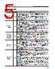
6 / 24 page  6/24 ¡ Semiconductor MSM66585/586/587/P587/Q587 PIN DESCRIPTIONS (Continued) Symbol Type Description P6_0/INT0 P6_1/INT1 P6_2/RXD1 P6_3/TXD1 P6_4/RXC1 P6_5/TXC1 Port 6 is 6 input/output pins. Input or output can be specified for each bit with the Port 6 Mode Register (P6IO). P6_0-P6_5 also have a secondary function as input/output pins for internal operation. Their secondary function can be set for each bit with the Port 6 Secondary Function Control Register (P6SF). The input/output settings of P6IO will be ignored for pins that have been set to the secondary function by P6SF. INT0 (P5_0), INT1 (P6_1): These pins input external interrupts 0 and 1. RXD1 (P6_2): This pin inputs receive data to the Serial Port 1 receive circuit. TXD1 (P6_3): This pin outputs transmit data to the Serial Port 1 transmit circuit. RXC1 (P6_4): This pin outputs the shift clock when the Serial Port 1 receive circuit is in master mode. It inputs the shift clock when the receive circuit is in slave mode. TXC1 (P6_4): This pin outputs the shift clock when the Serial Port 1 transmit circuit is in master mode. It inputs the shift clock when the transmit circuit is in slave mode. After reset (by RES signal input, BRK instruction execution, or op code trap), P6 will be high-impedance inputs. I/O P7_0/WR P7_1/RD P7_2/WAIT P7_3/CLKOUT P7_4/PWM0 P7_5-P7_7 Port 7 is 8 input/output pins. Input or output can be specified for each bit with the Port 7 Mode Register (P7IO). P7_0-P7_4 also have a secondary function as input/output pins for internal operation. Their secondary function can be set for each bit with the Port 7 Secondary Function Control Register (P7SF). The input/output settings of P7IO will be ignored for pins that have been set to the secondary function by P7SF. WR (P7_0): This pin outputs the strobe signal for write operations when external data memory is accessed. RD (P7_1): This pin outputs the strobe signal for read operations when external data memory is accessed. WAIT (P7_2): This pin inputs a wait to the internal CPU when external data memory with a slow access time is accessed. CPU is driven to "WAIT" state during WAIT pin high. CLKOUT (P7_3): This pin outputs the clock pulses set by the Peripheral Control Register (PRPHF). PWM0 (P7_4): This pin outputs PWM0. After reset (by RES signal input, BRK instruction execution, or op code trap), P7 will be high-impedance inputs. When P7_0 and P7_1 are used as their secondary functions (WR, RD), they need to be connected externally to pull-up resistors. I/O P8_0-P8_7 I/O Port 8 is 8 input/output pins. Input or output can be specified for each bit with the Port 8 Mode Register (P8IO). After reset (by RES signal input, BRK instruction execution, or op code trap), P8 will be high-impedance inputs. |
|
|
Link URL |
| Lei ha avuto il aiuto da alldatasheet? [ DONATE ] |
Di alldatasheet | Richest di pubblicita | contatti | Privacy Policy | Collegamento alla scheda tecnica | scambio Link | Ricerca produttore All Rights Reserved©Alldatasheet.com |
| Russian : Alldatasheetru.com | Korean : Alldatasheet.co.kr | Spanish : Alldatasheet.es | French : Alldatasheet.fr | Italian : Alldatasheetit.com Portuguese : Alldatasheetpt.com | Polish : Alldatasheet.pl | Vietnamese : Alldatasheet.vn Indian : Alldatasheet.in | Mexican : Alldatasheet.com.mx | British : Alldatasheet.co.uk | New Zealand : Alldatasheet.co.nz |
|
Family Site : ic2ic.com |
icmetro.com |
 Italian ▼
 English
 Chinese
 German
 Japanese
 Russian
 Korean
 Spanish
 French
 Italian
 Portuguese
 Polish
 Vietnamese
 Indian
 Mexican
 British
 New Zealand