|
Motore di ricerca datesheet componenti elettronici |
|
|
Motore di ricerca datesheet componenti elettronici |
|
AD9744ACP-PCBZ Scheda tecnica(PDF) 7 Page - Analog Devices |
|
|
|||||||||||||||||||||||||||||
AD9744ACP-PCBZ Scheda tecnica(HTML) 7 Page - Analog Devices |
|
|
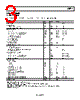
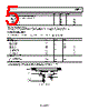
7 / 32 page  Data Sheet AD9744 Rev. C | Page 7 of 32 PIN CONFIGURATIONS AND FUNCTION DESCRIPTIONS Figure 3. 28-Lead SOIC and TSSOP Figure 4. 32-Lead LFCSP Table 6. Pin Function Descriptions SOIC/TSSOP Pin No. LFCSP Pin No. Mnemonic Description 1 27 DB13 Most Significant Data Bit (MSB). 2 to 13 28 to 32, 1, 2, 4 to 8 DB12 to DB1 Data Bits 12 to 1. 14 9 DB0 Least Significant Data Bit (LSB). 15 25 SLEEP Power-Down Control Input. Active high. Contains active pull-down circuit; it may be left unterminated if not used. 16 N/A REFLO Reference Ground when Internal 1.2 V Reference Used. Connect to ACOM for both internal and external reference operation modes. 17 23 REFIO Reference Input/Output. Serves as reference input when using external reference. Serves as 1.2 V reference output when using internal reference. Requires 0.1 µF capacitor to ACOM when using internal reference. 18 24 FS ADJ Full-Scale Current Output Adjust. 19 N/A NC No Internal Connection. 20 19, 22 ACOM Analog Common. 21 20 IOUTB Complementary DAC Current Output. Full-scale current when all data bits are 0s. 22 21 IOUTA DAC Current Output. Full-scale current when all data bits are 1s. 23 N/A RESERVED Reserved. Do not connect to common or supply. 24 17, 18 AVDD Analog Supply Voltage (3.3 V). 25 16 MODE Selects Input Data Format. Connect to DCOM for straight binary, DVDD for twos complement. N/A 15 CMODE Clock Mode Selection. Connect to CLKCOM for single-ended clock receiver (drive CLK+ and float CLK−). Connect to CLKVDD for differential receiver. Float for PECL receiver (terminations on-chip). 26 10, 26 DCOM Digital Common. 27 3 DVDD Digital Supply Voltage (3.3 V). 28 N/A CLOCK Clock Input. Data latched on positive edge of clock. N/A 12 CLK+ Differential Clock Input. N/A 13 CLK− Differential Clock Input. N/A 11 CLKVDD Clock Supply Voltage (3.3 V). N/A 14 CLKCOM Clock Common. N/A EPAD EPAD Exposed Pad. Connect the exposed pad thermally to a copper ground plane for enhanced electrical and thermal performance. 14 13 12 11 17 16 15 20 19 18 10 9 8 1 2 3 4 7 6 5 28 27 26 25 24 23 22 21 NC = NO CONNECT DB9 DB8 DB7 DB6 DB5 DB4 DB3 DB2 DB1 (LSB) DB0 CLOCK DVDD DCOM MODE AVDD RESERVED IOUTA IOUTB ACOM NC FS ADJ REFIO REFLO SLEEP DB10 DB11 DB12 (MSB) DB13 AD9744 TOP VIEW (Not to Scale) FS ADJ REFIO ACOM IOUTA DB7 NOTES 1. CONNECT THE EXPOSED PAD THERMALLY TO A COPPER GROUND PLANE FOR ENHANCED ELECTRICAL AND THERMAL PERFORMANCE. DB6 DVDD IOUTB ACOM AVDD AVDD DB5 DB4 DB3 DB2 DB1 24 23 22 21 20 19 18 17 1 2 3 4 5 6 7 8 AD9744 TOP VIEW (Not to Scale) |
|
Link URL |
| Lei ha avuto il aiuto da alldatasheet? [ DONATE ] |
Di alldatasheet | Richest di pubblicita | contatti | Privacy Policy | Collegamento alla scheda tecnica | scambio Link | Ricerca produttore All Rights Reserved©Alldatasheet.com |
| Russian : Alldatasheetru.com | Korean : Alldatasheet.co.kr | Spanish : Alldatasheet.es | French : Alldatasheet.fr | Italian : Alldatasheetit.com Portuguese : Alldatasheetpt.com | Polish : Alldatasheet.pl | Vietnamese : Alldatasheet.vn Indian : Alldatasheet.in | Mexican : Alldatasheet.com.mx | British : Alldatasheet.co.uk | New Zealand : Alldatasheet.co.nz |
|
Family Site : ic2ic.com |
icmetro.com |
 Italian ▼
 English
 Chinese
 German
 Japanese
 Russian
 Korean
 Spanish
 French
 Italian
 Portuguese
 Polish
 Vietnamese
 Indian
 Mexican
 British
 New Zealand