|
Motore di ricerca datesheet componenti elettronici |
|
|
Motore di ricerca datesheet componenti elettronici |
|
STLM75 Scheda tecnica(PDF) 25 Page - STMicroelectronics |
|
|
|||||||||||||||||||||||||||||
STLM75 Scheda tecnica(HTML) 25 Page - STMicroelectronics |
|
|
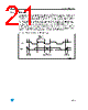
25 / 37 page  STLM75 Functional description 25/37 3.6 WRITE mode In this mode the master transmitter transmits to the STLM75 slave receiver. Bus protocol is shown in Figure 12. Following the START condition and slave address, a logic '0' (R/W = 0) is placed on the bus and indicates to the addressed device that word address will follow and is to be written to the on-chip address pointer. These modes are shown in the WRITE mode typical timing diagrams (see Figure 12, and Figure 13, and Figure 14). Figure 12. Typical pointer set followed by an immediate READ from the configuration register Figure 13. Configuration register WRITE AI12230 19 1 9 Repeat Start by Master ACK by STLM75 No ACK by STLM75 Stop Cond. by Master 1 0 0 1 A2 A1 A0 D7 D6 D5 D4 D3 D2 D1 D0 R/W Address Byte Data Byte 11 99 1 Start by Master Address Byte Pointer Byte ACK by STLM75 ACK by STLM75 0 0 1 A2 A1 A0 R/W 0 0 0 0 0 0 D1 D0 AI12231 11 99 1 9 1 Start by Master Address Byte Pointer Byte ACK by STLM75 ACK by STLM75 ACK by STLM75 Stop Cond. by Master 00 1 A2 A1 A0 R/W 00 0 0 0 0 0 0 0 D4 D3 D2 D1 D0 D1 D0 Configuration Byte |
|
Link URL |
| Lei ha avuto il aiuto da alldatasheet? [ DONATE ] |
Di alldatasheet | Richest di pubblicita | contatti | Privacy Policy | Collegamento alla scheda tecnica | scambio Link | Ricerca produttore All Rights Reserved©Alldatasheet.com |
| Russian : Alldatasheetru.com | Korean : Alldatasheet.co.kr | Spanish : Alldatasheet.es | French : Alldatasheet.fr | Italian : Alldatasheetit.com Portuguese : Alldatasheetpt.com | Polish : Alldatasheet.pl | Vietnamese : Alldatasheet.vn Indian : Alldatasheet.in | Mexican : Alldatasheet.com.mx | British : Alldatasheet.co.uk | New Zealand : Alldatasheet.co.nz |
|
Family Site : ic2ic.com |
icmetro.com |
 Italian ▼
 English
 Chinese
 German
 Japanese
 Russian
 Korean
 Spanish
 French
 Italian
 Portuguese
 Polish
 Vietnamese
 Indian
 Mexican
 British
 New Zealand