|
Motore di ricerca datesheet componenti elettronici |
|
|
Motore di ricerca datesheet componenti elettronici |
|
CC1010-RTY1 Scheda tecnica(PDF) 37 Page - Texas Instruments |
|
|
|||||||||||||||||||||||||||||
CC1010-RTY1 Scheda tecnica(HTML) 37 Page - Texas Instruments |
|
|
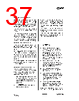
37 / 150 page  CC1010 SWRS047A Page 37 of 146 15.10 Flash Program Memory CC1010 has 32 kBytes of on-chip Flash program memory. It is divided into 256 pages of 128 bytes each. It can be programmed / erased through a serial SPI interface or page-by-page from the 8051 as described in the following sections. The endurance for the Flash program memory is typically 20.000 erase / write cycles. The Flash program memory can be locked for further reading / writing by setting appropriate lock bits through the serial interface. Chip erase must be performed to unlock the memory. This provides a way to prevent software from being copied by others. It can also prevent parts of the Flash memory from being modified by software, such as a boot loader that should remain unchanged. Other parts of the Flash may still be updated by the boot loader. For the security of the Flash protection, please refer to the disclaimer at the end of this document. Erasing a Flash page takes 10-20 ms depending on the FLTIM register. Writing to a Flash page takes 5-10 ms. 15.11 SPI Flash Programming The on-chip Flash program memory can be programmed using the SPI Flash programming protocol described in this section. SPI Flash programming is enabled when the pin PROG is held low. This enables the SPI slave, using the pins SCK (P0.0) as the clock input, SI (P0.1) as the serial data input and SO (P0.2) as the serial data output. A Windows based Flash programmer is also available free of charge at the Chipcon web site. 15.12 Serial Programming Algorithm When writing serial data to the SPI interface, data is clocked at the rising edge of SCK. When reading data from the SPI interface, data is clocked at the falling edge of SCK, see Figure 5. 1. Apply power between VDD and DGND while SCK is set to ‘0’. If a crystal is not connected between XOSC_Q1 and XOSC_Q2 apply a clock signal to the XOSC_Q1 pin. 2. Give RESET a negative pulse of at least one XOSC period. 3. Set PROG low. 4. Send the Programming Enable command. Check that the slave is synchronised by verifying that the second byte of the instruction is echoed back when issuing the third byte. If the second byte did not echo, issue a positive pulse on SCK and try again. In the worst case it will take 32 attempts to synchronise. 5. Send the Set Write Cycle Time command according to the device clock oscillator frequency. c*16*clock period must be between 20-40us for safe flash programming. 6. If a chip erase is performed wait 450ms after the instruction before issuing Write. 7. Flash memory is programmed one page at a time. Each page consists of 128 bytes. Load all bytes of the page that is to be programmed with the Load Program Memory Page instruction. 8. When all bytes of a page has been loaded issue Write Program Memory Page with the page address. The write operation finishes within 5.4ms. Reading an address while writing will return 0xFF. This can be used for polling |
|
Link URL |
| Lei ha avuto il aiuto da alldatasheet? [ DONATE ] |
Di alldatasheet | Richest di pubblicita | contatti | Privacy Policy | Collegamento alla scheda tecnica | scambio Link | Ricerca produttore All Rights Reserved©Alldatasheet.com |
| Russian : Alldatasheetru.com | Korean : Alldatasheet.co.kr | Spanish : Alldatasheet.es | French : Alldatasheet.fr | Italian : Alldatasheetit.com Portuguese : Alldatasheetpt.com | Polish : Alldatasheet.pl | Vietnamese : Alldatasheet.vn Indian : Alldatasheet.in | Mexican : Alldatasheet.com.mx | British : Alldatasheet.co.uk | New Zealand : Alldatasheet.co.nz |
|
Family Site : ic2ic.com |
icmetro.com |
 Italian ▼
 English
 Chinese
 German
 Japanese
 Russian
 Korean
 Spanish
 French
 Italian
 Portuguese
 Polish
 Vietnamese
 Indian
 Mexican
 British
 New Zealand