|
Motore di ricerca datesheet componenti elettronici |
|
|
Motore di ricerca datesheet componenti elettronici |
|
CM6800AGIP Scheda tecnica(PDF) 9 Page - Champion Microelectronic Corp. |
|
|
|||||||||||||||||||||||||||||
CM6800AGIP Scheda tecnica(HTML) 9 Page - Champion Microelectronic Corp. |
|
|
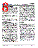
9 / 18 page  CM6800A LOW START-UP CURRENT PFC/PWM CONTROLLER COMBO 2009/08/10 Rev. 1.6 Champion Microelectronic Corporation Page 9 The output of the gain modulator is a current signal, in the form of a full wave rectified sinusoid at twice the line frequency. This current is applied to the virtual-ground (negative) input of the current error amplifier. In this way the gain modulator forms the reference for the current error loop, and ultimately controls the instantaneous current draw of the PFC form the power line. The general for of the output of the gain modulator is: IGAINMOD = 2 RMS AC V VEAO I × x 1V (1) More exactly, the output current of the gain modulator is given by: IGAINMOD = K x (VEAO – 0.625V) x IAC Where K is in units of V -1 Note that the output current of the gain modulator is limited around 228.47 μ A and the maximum output voltage of the gain modulator is limited to 228.47uA x 3.5K=0.8V. This 0.8V also will determine the maximum input power. However, IGAINMOD cannot be measured directly from ISENSE. ISENSE = IGAINMOD-IOFFSET and IOFFSET can only be measured when VEAO is less than 0.5V and IGAINMOD is 0A. Typical IOFFSET is around 60uA. Selecting RAC for IAC pin IAC pin is the input of the gain modulator. IAC also is a current mirror input and it requires current input. By selecting a proper resistor RAC, it will provide a good sine wave current derived from the line voltage and it also helps program the maximum input power and minimum input line voltage. RAC=Vin peak x 7.9K. For example, if the minimum line voltage is 80VAC, the RAC=80 x 1.414 x 7.9K=894Kohm. Current Error Amplifier, IEAO The current error amplifier’s output controls the PFC duty cycle to keep the average current through the boost inductor a linear function of the line voltage. At the inverting input to the current error amplifier, the output current of the gain modulator is summed with a current which results from a negative voltage being impressed upon the ISENSE pin. The negative voltage on ISENSE represents the sum of all currents flowing in the PFC circuit, and is typically derived from a current sense resistor in series with the negative terminal of the input bridge rectifier. In higher power applications, two current transformers are sometimes used, one to monitor the IF of the boost diode. As stated above, the inverting input of the current error amplifier is a virtual ground. Given this fact, and the arrangement of the duty cycle modulator polarities internal to the PFC, an increase in positive current from the gain modulator will cause the output stage to increase its duty cycle until the voltage on ISENSE is adequately negative to cancel this increased current. Similarly, if the gain modulator’s output decreases, the output duty cycle will decrease, to achieve a less negative voltage on the ISENSE pin. Cycle-By-Cycle Current Limiter and Selecting RS The ISENSE pin, as well as being a part of the current feedback loop, is a direct input to the cycle-by-cycle current limiter for the PFC section. Should the input voltage at this pin ever be more negative than –1V, the output of the PFC will be disabled until the protection flip-flop is reset by the clock pulse at the start of the next PFC power cycle. RS is the sensing resistor of the PFC boost converter. During the steady state, line input current x RS = IGAINMOD x 3.5K. Since the maximum output voltage of the gain modulator is IGAINMOD max x 3.5K= 0.8V during the steady state, RS x line input current will be limited below 0.8V as well. Therefore, to choose RS, we use the following equation: RS =0.8V x Vinpeak/(2x Line Input power) For example, if the minimum input voltage is 80VAC, and the maximum input rms power is 200Watt, RS = (0.8V x 80V x 1.414)/(2 x 200) = 0.226 ohm. PFC OVP In the CM6800A, PFC OVP comparator serves to protect the power circuit from being subjected to excessive voltages if the load should suddenly change. A resistor divider from the high voltage DC output of the PFC is fed to VFB. When the voltage on VFB exceeds 2.75V, the PFC output driver is shut down. The PWM section will continue to operate. The OVP comparator has 250mV of hysteresis, and the PFC will not restart until the voltage at VFB drops below 2.50V. The VFB power components and the CM6800A are within their safe operating voltages, but not so low as to interfere with the boost voltage regulation loop. Also, VCC OVP can be served as a redundant PFCOVP protection. VCC OVP threshold is 17.9V with 1.5V hysteresis. |
|
|
Link URL |
| Lei ha avuto il aiuto da alldatasheet? [ DONATE ] |
Di alldatasheet | Richest di pubblicita | contatti | Privacy Policy | Collegamento alla scheda tecnica | scambio Link | Ricerca produttore All Rights Reserved©Alldatasheet.com |
| Russian : Alldatasheetru.com | Korean : Alldatasheet.co.kr | Spanish : Alldatasheet.es | French : Alldatasheet.fr | Italian : Alldatasheetit.com Portuguese : Alldatasheetpt.com | Polish : Alldatasheet.pl | Vietnamese : Alldatasheet.vn Indian : Alldatasheet.in | Mexican : Alldatasheet.com.mx | British : Alldatasheet.co.uk | New Zealand : Alldatasheet.co.nz |
|
Family Site : ic2ic.com |
icmetro.com |
 Italian ▼
 English
 Chinese
 German
 Japanese
 Russian
 Korean
 Spanish
 French
 Italian
 Portuguese
 Polish
 Vietnamese
 Indian
 Mexican
 British
 New Zealand