|
Motore di ricerca datesheet componenti elettronici |
|
|
Motore di ricerca datesheet componenti elettronici |
|
HT47C20 Scheda tecnica(PDF) 5 Page - Holtek Semiconductor Inc |
|
|
|||||||||||||||||||||||||||||
HT47C20 Scheda tecnica(HTML) 5 Page - Holtek Semiconductor Inc |
|
|
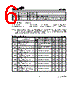
5 / 56 page  Pad Description Pad No. Pad Name I/O Mask Option Function 1 RES I ¾ Schmitt trigger reset input. Active low. 2 3 4 5 6~9 PA0/BZ PA1/BZ PA2/IR PA3/PFD PA4~PA7 I/O Wake-up Pull-high or None CMOS or NMOS Bidirectional 8-bit input/output port. The low nibble of the PA can be configured as CMOS output or NMOS output with or without pull-high resistors (mask option). NMOS output can be configured as schmitt trigger input with or without pull-high resis- tors. Each bit of NMOS output can be configured as wake up input by mask option. Of the eight bits, PA0~PA1 can be set as I/O pins or buzzer outputs by mask option. PA2 can be set as an I/O pin or an IR carrier output also by mask option. PA3 can be set as an I/O pin or a PFD output also by mask option. 10 11 12 13 PB0/INT PB1 PB2/TMR PB3 I ¾ Four-bit Schmitt trigger input port. The PB is config- ured as with pull-high resistors. Of the four bits, PB0 can be set as an input pin or an external interrupt in- put pin (INT) by software application. While PB2 can be set as an input pin or a timer/event counter input pin also by software application. 14 VSS ¾¾ Negative power supply, GND 18 17 16 15 IN1 CS1 RS1 RT1 I O O O ¾ Oscillation input pin of channel 1 Reference capacitor connection pin of channel 1 Reference resistor connection pin of channel 1 Resistor sensor connection pin for measurement of channel 1 23 22 21 20 19 IN0 CS0 RS0 CRT0 RT0 I O O O O ¾ Oscillation input pin of channel 0 Reference capacitor connection pin of channel 0 Reference resistor connection pin of channel 0 Resistor/capacitor sensor connection pin for mea- surement of channel 0 Resistor sensor connection pin for measurement of channel 0 27 26~24 SEG19/COM3 COM2~COM0 O 1/3 or 1/4 Duty SEG19/COM3 can be set as a segment or a common output driver for LCD panel by mask option. COM2~COM0 are outputs for LCD panel plate. 28~46 SEG18~SEG0 O ¾ LCD driver outputs for LCD panel segments 49, 48, 47 51, 50 V1, V2, V3 C1, C2 ¾¾ Voltage pump 52 53 OSC4 OSC3 O I ¾ Real time clock oscillators HT47C20 5 January 18, 2000 |
|
Link URL |
| Lei ha avuto il aiuto da alldatasheet? [ DONATE ] |
Di alldatasheet | Richest di pubblicita | contatti | Privacy Policy | Collegamento alla scheda tecnica | scambio Link | Ricerca produttore All Rights Reserved©Alldatasheet.com |
| Russian : Alldatasheetru.com | Korean : Alldatasheet.co.kr | Spanish : Alldatasheet.es | French : Alldatasheet.fr | Italian : Alldatasheetit.com Portuguese : Alldatasheetpt.com | Polish : Alldatasheet.pl | Vietnamese : Alldatasheet.vn Indian : Alldatasheet.in | Mexican : Alldatasheet.com.mx | British : Alldatasheet.co.uk | New Zealand : Alldatasheet.co.nz |
|
Family Site : ic2ic.com |
icmetro.com |
 Italian ▼
 English
 Chinese
 German
 Japanese
 Russian
 Korean
 Spanish
 French
 Italian
 Portuguese
 Polish
 Vietnamese
 Indian
 Mexican
 British
 New Zealand