|
Motore di ricerca datesheet componenti elettronici |
|
|
Motore di ricerca datesheet componenti elettronici |
|
HTG1390 Scheda tecnica(PDF) 7 Page - Holtek Semiconductor Inc |
|
|
|||||||||||||||||||||||||||||
HTG1390 Scheda tecnica(HTML) 7 Page - Holtek Semiconductor Inc |
|
|
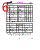
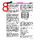
7 / 27 page  Mode Program Counter PC11 PC10 PC9 PC8 PC7 PC6 PC5 PC4 PC3 PC2 PC1 PC0 Initial reset 0 0 0 0 0 0 0 0 0 0 0 0 Internal interrupt 0 0 0 0 0 0 0 0 0 1 0 0 External interrupt 0 0 0 0 0 0 0 0 1 0 0 0 Jump, call instruction P11 P10 P9 P8 P7 P6 P5 P4 P3 P2 P1 P0 Conditional branch @ P10 P9 P8 P7 P6 P5 P4 P3 P2 P1 P0 Return from subroutine S11 S10 S9 S8 S7 S6 S5 S4 S3 S2 S1 S0 Program memory System Architecture Program counter – PC This counter addresses the program ROM and is arranged as an 12-bit binary counter from PC0 to PC11 whose contents specify a maxi- mum of 4096 addresses. The program counter counts with an increment of 1 or 2 with each execution of an instruction. When executing the jump instruction (JMP, JNZ, JC, JTMR,...), a subroutine call, initial reset, internal interrupt, external interrupt or returning from a subroutine, the program counter is loaded with the corresponding in- struction data as shown in the table. Notes: P0~P11: Instruction code @: PC11 keeps current value S0~S11: Stack register bits Program memory – ROM The program memory is the executable memory and is arranged in a 4096 ×8 bit format. The address is specified by the program counter (PC). Four special locations are reserved as de- scribed as follows. • Location 0 Activating the processor RES pin causes the first instruction to be fetched from location 0. • Location 4 Contains the timer interrupt resulting from a TIMER overflow. If the interrupts are enabled it causes the program to jump to this subroutine. • Location 8 Activating the PS or PP input pins of the processor with the interrupts enabled during Halt mode causes the program to jump to this location. • Locations n00H to nFFH These are the 256 bytes of each page in pro- gram memory. This area from n00H to nFFH and F00H to FFFH can be used as a look–up table. Instructions such as READ R4A, READ MR0A, READF R4A, READF MR0A can read the table and transfer the contents of the table to ACC and R4 or to ACC and a data memory address specified by the register pair R1,R0. However as R1,R0 can only store 8 bits, these instructions cannot fully specify the full 12 bit program memory address. For this reason a jump instruction should be first used to place the program counter in the right page. The above instructions can then be used to read the look up table data. Program memory HTG1390 Preliminary 7 17th Nov ’98 |
|
Link URL |
| Lei ha avuto il aiuto da alldatasheet? [ DONATE ] |
Di alldatasheet | Richest di pubblicita | contatti | Privacy Policy | Collegamento alla scheda tecnica | scambio Link | Ricerca produttore All Rights Reserved©Alldatasheet.com |
| Russian : Alldatasheetru.com | Korean : Alldatasheet.co.kr | Spanish : Alldatasheet.es | French : Alldatasheet.fr | Italian : Alldatasheetit.com Portuguese : Alldatasheetpt.com | Polish : Alldatasheet.pl | Vietnamese : Alldatasheet.vn Indian : Alldatasheet.in | Mexican : Alldatasheet.com.mx | British : Alldatasheet.co.uk | New Zealand : Alldatasheet.co.nz |
|
Family Site : ic2ic.com |
icmetro.com |
 Italian ▼
 English
 Chinese
 German
 Japanese
 Russian
 Korean
 Spanish
 French
 Italian
 Portuguese
 Polish
 Vietnamese
 Indian
 Mexican
 British
 New Zealand