|
Motore di ricerca datesheet componenti elettronici |
|
|
Motore di ricerca datesheet componenti elettronici |
|
HTG1390 Scheda tecnica(PDF) 8 Page - Holtek Semiconductor Inc |
|
|
|||||||||||||||||||||||||||||
HTG1390 Scheda tecnica(HTML) 8 Page - Holtek Semiconductor Inc |
|
|
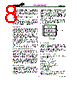
8 / 27 page  Note that the page number n must be greater than zero as some locations in page 0 are re- served for specific usage as mentioned. This area may function as normal program memory as required. The program memory mapping is shown in the diagram. In the execution of an instruction the program counter is added before the execution phase, so careful manipulation of READ MR0A and READ R4A is needed in the page margin. Stack register The stack register is a group of registers used to save the contents of the program counter (PC) and is arranged in 13 bits ×1 level. One bit is used to store the carry flag. An interrupt will force the contents of the PC and the carry flag onto the stack register. A subroutine call will also cause the PC contents to be pushed onto the stack; however the carry flag will not be stored. At the end of a subroutine or an inter- rupt (indicated by a return instruction RET or RETI), the contents of the stack register are returned to the PC. Executing “RETI” instruction will restore the carry flag from stack register, but “RET” doesn’t. Working registers – R0,R1,R2,R3,R4 There are 5 working registers (R0,R1,R2,R3, R4) usually used to store the frequently ac- cessed intermediate results. Using the instruc- tions INC Rn and DEC Rn the working registers can increment (+1) or decrement (–1). The JNZ Rn (n=0,1,4) instruction makes effi- cient use of the working registers as a program loop counter. Also the register pairs R0,R1 and R2,R3 are used as a data memory pointer when the memory transfer instruction is executed. Data memory – RAM The static data memory (RAM) is arranged in 256 ×4 bit format and is used to store data. All of the data memory locations are indirectly ad- dressable through the register pair R1,R0 or R3,R2; for example MOV A,[R3R2] or MOV [R3R2],A. There are two areas in the data memory, the temporary data area and the display data area. Access to the temporary data area is from 00H to 7FH. Locations E0H to FAH represent the display data area. The locations between the temporary and display data areas are unde- fined and cannot be used. When data is written into the display data area it is automatically read by the LCD driver which then generates the corresponding LCD driving signals. Accumulator – ACC The accumulator is the most important data register in the processor. It is one of the sources of input to the ALU and the destination of the results of the operations performed in the ALU. Data to and from the I/O ports and memory also passes through the accumulator. Arithmetic and logic unit – ALU This circuit performs the following arithmetic and logical operations ... • Add with or without carry • Subtract with or without carry • AND, OR, Exclusive-OR • Rotate right, left through carry • BCD decimal adjust for addition • Increment, decrement • Data transfers • Branch decisions The ALU not only outputs the results of data operations, but also sets the status of the carry flag (CF) in some instructions. Data memory HTG1390 Preliminary 8 17th Nov ’98 |
|
Link URL |
| Lei ha avuto il aiuto da alldatasheet? [ DONATE ] |
Di alldatasheet | Richest di pubblicita | contatti | Privacy Policy | Collegamento alla scheda tecnica | scambio Link | Ricerca produttore All Rights Reserved©Alldatasheet.com |
| Russian : Alldatasheetru.com | Korean : Alldatasheet.co.kr | Spanish : Alldatasheet.es | French : Alldatasheet.fr | Italian : Alldatasheetit.com Portuguese : Alldatasheetpt.com | Polish : Alldatasheet.pl | Vietnamese : Alldatasheet.vn Indian : Alldatasheet.in | Mexican : Alldatasheet.com.mx | British : Alldatasheet.co.uk | New Zealand : Alldatasheet.co.nz |
|
Family Site : ic2ic.com |
icmetro.com |
 Italian ▼
 English
 Chinese
 German
 Japanese
 Russian
 Korean
 Spanish
 French
 Italian
 Portuguese
 Polish
 Vietnamese
 Indian
 Mexican
 British
 New Zealand