|
Motore di ricerca datesheet componenti elettronici |
|
|
Motore di ricerca datesheet componenti elettronici |
|
AT86RF211DAI-R Scheda tecnica(PDF) 24 Page - ATMEL Corporation |
|
|
|||||||||||||||||||||||||||||
AT86RF211DAI-R Scheda tecnica(HTML) 24 Page - ATMEL Corporation |
|
|
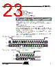
24 / 48 page  24 AT86RF211 1942C–WIRE–06/02 Only the 2 MSBs are updated on the rising edge of SLE; other register bits are unchanged. • READ Mode (R/W = 0) The address and R/W bits are clocked on the rising edge of SCK. The data bits are changed on the falling edge of SCK. The MSB of the register is the first bit read. SDATA I/O pin is switched from input to output on the edge following the "1" clocking the R/W bit. It is possible to stop reading a register (SLE back to “1”)at any time. If an attempt to read more bits than the register capacity is detected, SDATA is clamped to “0”. If the address of a register is not valid, SDATA is set to “1” during the first 32 SCK peri- ods, then to “0” during all the extra periods. SDATA is switched back to the input state when SLE is back to “1”. Figure 31. Read Chronogram: Complete Read Cycle from a 10 bits Register Figure 32. Read chronogram: Partial Read Cycle, Reading 2 bits A[0] D[9 ] D[8] A[1] A[2 ] D[7] A[3] R/W SLE SCK SDATA D[6] D[5] D[4] D[3] D[2] D[1] D[0] INPUT OUTPUT INPUT SDATA direction A[0] D[31] A[1] A[2] A[3] R/W SLE SCK SDATA SDATA mode INPUT D[30] OUTPUT INPUT |
|
Link URL |
| Lei ha avuto il aiuto da alldatasheet? [ DONATE ] |
Di alldatasheet | Richest di pubblicita | contatti | Privacy Policy | Collegamento alla scheda tecnica | scambio Link | Ricerca produttore All Rights Reserved©Alldatasheet.com |
| Russian : Alldatasheetru.com | Korean : Alldatasheet.co.kr | Spanish : Alldatasheet.es | French : Alldatasheet.fr | Italian : Alldatasheetit.com Portuguese : Alldatasheetpt.com | Polish : Alldatasheet.pl | Vietnamese : Alldatasheet.vn Indian : Alldatasheet.in | Mexican : Alldatasheet.com.mx | British : Alldatasheet.co.uk | New Zealand : Alldatasheet.co.nz |
|
Family Site : ic2ic.com |
icmetro.com |
 Italian ▼
 English
 Chinese
 German
 Japanese
 Russian
 Korean
 Spanish
 French
 Italian
 Portuguese
 Polish
 Vietnamese
 Indian
 Mexican
 British
 New Zealand