 |
Motore di ricerca datesheet componenti elettronici |
|
|
Motore di ricerca datesheet componenti elettronici |
|
The question interval is too short.
Please try again in a few seconds.

Hello, Please ask a question about AD9744 Datasheet
# Example questions:
➢ What is the minimum acceptable latch pulse width (tlpw)?
➢ What is the typical value for the input hold time (th) for the digital inputs?
➢ The document mentions a 'multitone power ratio'. what frequency range is used to measure this ratio in the given example?
| Part No. | AD9744 |
| Manufacturer | AD |
| Size | 1Mb |
| Pages | 32 pages |
| Description | 14-Bit, 210 MSPS TxDAC짰 D/A Converter |



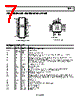








1. General Information (Revision B)
️· Device: AD9744
️· Datasheet Section Focus: These are excerpts focusing on Digital Specs, Analog Specs and Timing Specifications.
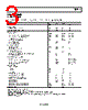
2. Digital Specifications
️· Digital Inputs (DB0–DB13):
- Logic 1 Voltage: 2.1V
- Logic 0 Voltage: 3V
- Logic 1 Current: 0 µA
- Logic 0 Current: 0.9 µA
- Input Capacitance: -10 to +10 pF
- Input Setup Time (tS): -10 to +10 ns
- Input Hold Time (tH): 5 to 2.0 ns
- Latch Pulse Width (tLPW): 1.5 ns
️· Clock Inputs (CLK+ & CLK– – applicable in differential or PECL mode):
- Input Voltage Range: 0 to 3 V
- Common-Mode Voltage: 0.75 V
- Differential Voltage: 1.5 to 2.25 V
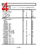
3. Analog and Timing Specifications
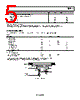
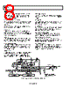
️· Analog Output (IOUTA or IOUTB): The details are somewhat incomplete here. This section refers to a Figure 2 that is not provided but describes timing. The descriptions use "0.1%" descriptions of timing elements, but the description of what the 0.1% is applied to is missing.
️· Timing Specifications (referencing Figure 2, not included):
- tS (Setup Time)
- tH (Hold Time)
- tPD (Propagation Delay)
- tLPW (Latch Pulse Width)
- tST (Settling Time)
4. Table Summaries (from the provided excerpts):
️· Table 0.1% (not numbered) – This table appears to be used for multiple values. A table structure is indicated using three columns, and multiple timing specifications are referenced.
️· Table 3 (Digital Specifications): Summarized above.
Key Limitations & Notes:
️· Missing Figure 2: The timing information heavily relies on Figure 2, which is not included. Without it, the precise meaning and values for timing parameters (tS, tH, tPD, tLPW, tST) cannot be fully understood.
️· Incomplete Analog Output Section: The section describing IOUTA/IOUTB is cut off, leaving details missing.
️· Table Numbering: The tables aren't consistently numbered in the extracts.
️· Context is Important: This information is best understood within the full AD9744 datasheet. The provided extracts are snippets, and some values might have specific conditions or caveats that are only clarified in the complete document.
1. General Information (Revision B)
️· Device: AD9744
️· Datasheet Section Focus: These are excerpts focusing on Digital Specs, Analog Specs and Timing Specifications.
2. Digital Specifications
️· Digital Inputs (DB0–DB13):
- Logic 1 Voltage: 2.1V
- Logic 0 Voltage: 3V
- Logic 1 Current: 0 µA
- Logic 0 Current: 0.9 µA
- Input Capacitance: -10 to +10 pF
- Input Setup Time (tS): -10 to +10 ns
- Input Hold Time (tH): 5 to 2.0 ns
- Latch Pulse Width (tLPW): 1.5 ns
️· Clock Inputs (CLK+ & CLK– – applicable in differential or PECL mode):
- Input Voltage Range: 0 to 3 V
- Common-Mode Voltage: 0.75 V
- Differential Voltage: 1.5 to 2.25 V
3. Analog and Timing Specifications
️· Analog Output (IOUTA or IOUTB): The details are somewhat incomplete here. This section refers to a Figure 2 that is not provided but describes timing. The descriptions use "0.1%" descriptions of timing elements, but the description of what the 0.1% is applied to is missing.
️· Timing Specifications (referencing Figure 2, not included):
- tS (Setup Time)
- tH (Hold Time)
- tPD (Propagation Delay)
- tLPW (Latch Pulse Width)
- tST (Settling Time)
4. Table Summaries (from the provided excerpts):
️· Table 0.1% (not numbered) – This table appears to be used for multiple values. A table structure is indicated using three columns, and multiple timing specifications are referenced.
️· Table 3 (Digital Specifications): Summarized above.
Key Limitations & Notes:
️· Missing Figure 2: The timing information heavily relies on Figure 2, which is not included. Without it, the precise meaning and values for timing parameters (tS, tH, tPD, tLPW, tST) cannot be fully understood.
️· Incomplete Analog Output Section: The section describing IOUTA/IOUTB is cut off, leaving details missing.
️· Table Numbering: The tables aren't consistently numbered in the extracts.
️· Context is Important: This information is best understood within the full AD9744 datasheet. The provided extracts are snippets, and some values might have specific conditions or caveats that are only clarified in the complete document.
| Part No. | AD9744 |
| Manufacturer | AD |
| Size | 1Mb |
| Pages | 32 pages |
| Description | 14-Bit, 210 MSPS TxDAC짰 D/A Converter |
| Lei ha avuto il aiuto da alldatasheet? [ DONATE ] |
Di alldatasheet | Richest di pubblicita | contatti | Privacy Policy | Collegamento alla scheda tecnica | scambio Link | Ricerca produttore All Rights Reserved©Alldatasheet.com |
| Russian : Alldatasheetru.com | Korean : Alldatasheet.co.kr | Spanish : Alldatasheet.es | French : Alldatasheet.fr | Italian : Alldatasheetit.com Portuguese : Alldatasheetpt.com | Polish : Alldatasheet.pl | Vietnamese : Alldatasheet.vn Indian : Alldatasheet.in | Mexican : Alldatasheet.com.mx | British : Alldatasheet.co.uk | New Zealand : Alldatasheet.co.nz |
|
Family Site : ic2ic.com |
icmetro.com |
 Italian ▼
  English
 Chinese
 German
 Japanese
 Russian
 Korean
 Spanish
 French
 Portuguese
 Polish
 Vietnamese
 Indian
 Mexican
 British
 New Zealand